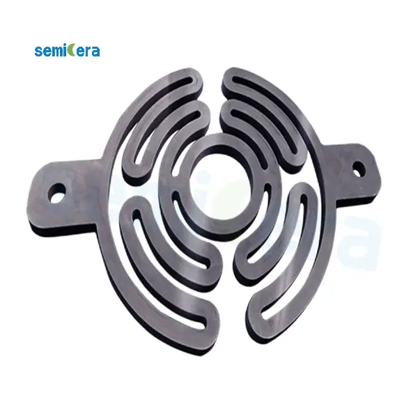
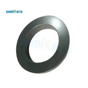
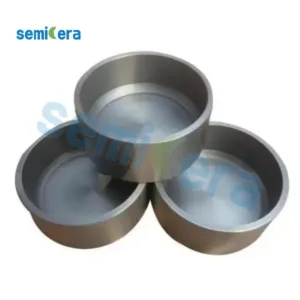
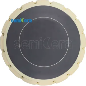
How Epitaxial Layers Shape the Future of Semiconductor Technology

News - Why Semiconductor Devices Require an “Epitaxial Layer”

You see how the Semiconductor Epitaxial Layer changes what you expect from electronics. When you use devices built on an Epitaxial (EPI) Silicon Wafer or a Single Crystal Germanium Wafer, you notice faster speeds and better reliability. These materials help you reach new heights in technology.

Key Takeaways

  • Epitaxial layers are thin, high-purity films grown on semiconductor wafers that improve device speed and reliability by reducing defects.
  • These layers allow precise control over material properties, leading to better energy efficiency, higher voltage tolerance, and longer device life.
  • Using epitaxial layers enables new device designs and advanced technologies, shaping the future of faster, stronger, and more efficient electronics.

The Transformative Role of Semiconductor Epitaxial Layer

The Transformative Role of Semiconductor Epitaxial Layer

What Is a Semiconductor Epitaxial Layer?

You may wonder what a Semiconductor Epitaxial Layer is. This layer is a thin, crystal-like film that grows on top of a wafer. You can think of it as a special coating that matches the structure of the base material. Scientists use advanced methods to create this layer, such as chemical vapor deposition. The atoms in the layer line up perfectly with the atoms in the wafer below. This careful alignment gives you a material with fewer defects and better performance.

Tip: When you use devices with a high-quality epitaxial layer, you get faster speeds and more reliable results.

Epitaxial Layer vs. Substrate: Key Differences

You might ask how the epitaxial layer differs from the substrate. The substrate is the original wafer, often made from silicon or another semiconductor. It acts as the foundation. The epitaxial layer sits on top of this base. Here is a simple table to help you see the differences:

Feature Substrate Epitaxial Layer
Location Bottom/base On top of substrate
Purpose Support and structure Improve device properties
Purity Standard Higher
Customization Limited Highly customizable

You can see that the epitaxial layer gives you more control over the final device. You can change its thickness, purity, and even its electrical properties.

Why Epitaxial Layers Matter for Device Quality

You want your electronic devices to work well and last long. The Semiconductor Epitaxial Layer plays a big role in this. It reduces the number of defects in the material. Fewer defects mean that electricity flows more smoothly. This leads to better performance and less heat. You also get devices that can handle higher voltages and work in tougher conditions.

  • You get higher speeds in your processors.
  • You see better energy efficiency in your power devices.
  • You notice longer lifespans for your electronics.

When you choose devices built with a high-quality epitaxial layer, you invest in technology that pushes the limits of what is possible.

Solving Challenges and Enabling Innovation with Epitaxial Layers

Overcoming Material Defects and Enhancing Purity

You want your electronic devices to work smoothly and last longer. One big challenge in making semiconductors is dealing with defects in the material. These defects can slow down your device or even cause it to fail. When you use a Semiconductor Epitaxial Layer, you help solve this problem. This layer grows in a controlled way, so it has fewer defects than the base wafer. You get a cleaner and more perfect crystal structure.

Note: Fewer defects mean better performance and higher reliability for your devices.

You also need high purity in your materials. Impurities can block the flow of electricity or cause unwanted reactions. The process of making a Semiconductor Epitaxial Layer lets you control the purity very closely. You can remove unwanted atoms and add only the elements you need. This control helps you build devices that work faster and use less energy.

Achieving High Breakdown Voltage and Device Efficiency

You may want your devices to handle high voltages without breaking down. The breakdown voltage is the point where a device fails because too much electricity passes through. With a high-quality epitaxial layer, you can increase this limit. The layer acts as a barrier that stops electricity from leaking or causing damage.

Here are some ways epitaxial layers help you achieve better efficiency and higher breakdown voltage:

  • You can make the layer thicker or thinner, depending on what your device needs.
  • You can adjust the amount of doping, which means adding special atoms to change how electricity flows.
  • You can create a smooth transition between different parts of your device.

Benefit How Epitaxial Layer Helps
Higher breakdown voltage Reduces weak spots in the crystal
Better efficiency Lowers energy loss
Longer device life Prevents early failure

When you use these features, you get devices that are safer and more efficient. Power electronics, like those in electric cars or solar panels, rely on these improvements.

Supporting Advanced Architectures and Novel Devices

You want to see new and exciting technology in your hands. The Semiconductor Epitaxial Layer makes this possible. It lets you build advanced device structures that were not possible before. For example, you can stack different layers with unique properties. You can also create very thin layers for tiny transistors or sensors.

Some innovations you can achieve with epitaxial layers include:

  • Multi-layer chips for faster computing
  • Sensors that detect light or chemicals with high accuracy
  • Power devices that work at higher temperatures

Tip: When you use epitaxial layers, you open the door to new designs and better performance.

You help shape the future of electronics by choosing devices built with these advanced layers. The technology keeps growing, and you will see even more powerful and creative devices soon.

Future Trends in Semiconductor Epitaxial Layer Technology

MERSEN epitaxy solutions | Silicon carbide for semiconductors

Emerging Materials and Growth Techniques

You will see new materials change the way you use electronics. Gallium nitride (GaN) and silicon carbide (SiC) now help you build faster and stronger devices. These materials let you make chips that work at higher temperatures and voltages. You can also use new growth techniques like molecular beam epitaxy and atomic layer deposition. These methods give you better control over the thickness and quality of each layer.

Note: When you use these advanced materials and methods, you get devices that last longer and work better.

Impact on Next-Generation Semiconductor Devices

You will notice big changes in your devices. Phones, computers, and cars will all benefit from these new layers. You can expect faster processors and better battery life. Power devices will become smaller and more efficient. Sensors will detect things more accurately. The Semiconductor Epitaxial Layer helps you reach these new levels of performance.

Device Type Improvement You See
Smartphones Faster speeds, less heat
Electric Vehicles Longer range, safer parts
Solar Panels Higher energy output

Opportunities and Challenges Ahead

You have many opportunities with these new technologies. You can design smaller, smarter, and more powerful devices. You will also face challenges. Making these layers costs more money and needs special tools. You must learn new skills to work with new materials. If you solve these problems, you will help shape the future of electronics.

Tip: Stay curious and keep learning about new materials and methods. You will lead the way in technology.


You now see how advanced layers help you shape the future of electronics. These layers let you design faster, stronger, and more reliable devices.

As you learn more, you will discover new ways to use these materials and lead the next wave of technology.

FAQ

What is the main benefit of using an epitaxial layer?

You get fewer defects in your device. This means your electronics work better and last longer.

Tip: High-quality epitaxial layers help you achieve faster speeds and better reliability.

Can you use epitaxial layers with materials other than silicon?

Yes, you can use them with materials like gallium nitride or silicon carbide. These materials help you build stronger and faster devices.

How do epitaxial layers improve energy efficiency?

You control the purity and thickness of the layer. This reduces energy loss and helps your device use less power.

Share:

More Posts

Send Us A Message

en_USEnglish