
Why SOS Wafers Eliminate the RF Substrate Loss That Silicon Can’t Avoid?
Every RF front-end designer eventually runs into the same wall: no matter how advanced the device layer process is, the substrate underneath the transistors quietly shapes insertion loss, isolation, and linearity. Conventional silicon — even the high-resistivity kind — was never built to be electrically transparent at gigahertz frequencies. Silicon-on-sapphire (SOS) wafer technology solves this at the material level instead of trying to engineer around it, which is exactly why it has held a durable position in RF switches and front-end modules for more than two decades.
1. What Is Substrate Loss, and Why Can’t Silicon Avoid It?
Bulk silicon wafers used for standard CMOS run around 10 Ω·cm — conductive enough for transistor operation, but also conductive enough to bleed RF energy into the substrate through eddy currents. That leakage shows up as insertion loss, reduced isolation between switch ports, and harmonic distortion that worsens with frequency.
The obvious fix looks like high-resistivity silicon (HR-Si), which pushes resistivity up to 10³–10⁴ Ω·cm. In practice, HR-Si only gets you partway there. Fixed positive charge at the SiO₂/Si interface forms a thin, uncontrolled conductive layer — an inversion or accumulation channel — that behaves electrically like a much lower-resistivity material. Subsequent thermal processing steps also generate donors at the buried interface and on the wafer backside, further degrading resistivity over time. The datasheet says resistive; at RF frequencies, the substrate doesn’t behave that way.
Resistivity Doesn’t Tell the Whole Story
|
Substrate |
Bulk Resistivity |
RF Behavior |
|
Standard bulk silicon |
~10 Ω·cm |
High loss, strong parasitic coupling |
|
High-resistivity silicon (HR-Si) |
~10³–10⁴ Ω·cm |
Improved, but surface conductive layer still leaks RF energy |
|
Trap-rich silicon |
Effectively several kΩ·cm |
Works well for many RF-SOI designs; trap layer suppresses parasitic-layer effects |
|
Sapphire (Al₂O₃) |
~10¹⁴ Ω·cm |
Best RF performance of the three; no comparable interface conduction layer |
2. Why Does Sapphire Solve This at the Material Level?
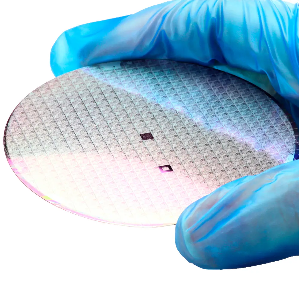
SOS wafers are made by epitaxially growing a thin single-crystal silicon layer on a single-crystal sapphire substrate — typically well under 150 nm in RF-optimized processes. Because sapphire’s insulating behavior comes from its band structure rather than from doping or process artifacts, there’s no equivalent thermal-donor generation to worry about, and no fixed-charge conduction channel to manage. The insulation is an inherent material property, not something that has to be re-verified after every thermal cycle.
Sapphire also brings RF advantages that go beyond resistivity: a relative dielectric constant of about 9.39 and a loss tangent below 10⁻⁴ at 3 GHz, both of which keep dielectric losses low well into millimeter-wave frequencies. Its thermal conductivity (~46 W/m·K) is far higher than SiO₂ (~1.4 W/m·K), which helps manage self-heating in thin-film devices — though it’s still notably lower than silicon’s own thermal conductivity, a tradeoff covered in Section 5.
This secondary advantage shows up more in aerospace and defense datasheets than in consumer parts: SOS and SOI structures offer better radiation tolerance than bulk silicon because the sensitive charge-collection region is confined to a thin, isolated film. Published space-grade SOS/SOI IC data shows dose-rate-sensitive volumes roughly two orders of magnitude smaller than equivalent bulk-silicon devices.
3. SOS vs. HR-Si vs. Trap-Rich SOI: How the RF Numbers Actually Compare
Comparative studies of insertion loss, harmonic generation, and Q factor across sapphire, trap-rich silicon, and HR-Si substrates for RF-SOI applications produce a consistent ranking: sapphire delivers the best RF performance; trap-rich silicon is limited but workable, with effective resistivity in the low kΩ·cm range; and HR-Si trails both, held back by parasitic conduction that the material itself can’t suppress.
Real device data backs this up. Published specs for silicon-on-sapphire CMOS RF switches show insertion loss of 0.38 dB in transmit mode and 0.5 dB in receive mode at 0.9 GHz, with second- and third-harmonic suppression of −91 dBc and −84 dBc respectively at +28 dBm input power — numbers that are difficult to match at the same power levels on bulk or unoptimized HR-Si substrates, since substrate-coupled harmonics tend to worsen with input power on lossier substrates.
Where Each Substrate Tends to Land
|
Metric |
HR-Si |
Trap-Rich Silicon |
SOS (Sapphire) |
|
Insertion loss |
Highest |
Moderate |
Lowest |
|
Harmonic distortion |
Worst — unsuppressed parasitic conduction |
Improved via trap layer |
Best — no comparable conduction path |
|
Port-to-port isolation |
Limited by substrate coupling |
Better |
Highest |
|
Process maturity / cost |
Lowest cost, most mature |
Adds a trap-layer process step |
Higher cost, requires heteroepitaxy |
4. Where Do SOS Wafers Actually Earn Their Keep?
● RF switches and antenna tuners: A fully insulating substrate lowers both on-resistance and parasitic substrate capacitance simultaneously — exactly what’s needed for the high-isolation, low-insertion-loss switch architectures used in smartphone front-end modules and Wi-Fi/5G switch banks.
● LNAs and mixers: Lower substrate coupling loss and crosstalk directly improve noise figure and channel-to-channel isolation in multi-port front-end designs.
● Radiation-hardened and aerospace electronics: A thin, isolated device layer shrinks the charge-collection volume exposed to single-event effects, which is why SOS still holds a solid position in satellite and defense electronics even as commercial-volume production has shifted toward SOI.
● MEMS and photonic integration: Sapphire’s optical transparency and chemical stability make it a good platform for co-locating RF or CMOS layers with optical or mechanical structures on the same substrate.
5. What Tradeoffs Should Buyers Know Before Specifying SOS?
The heteroepitaxial growth process that gives SOS its isolation advantage also creates a defect-dense region near the silicon/sapphire interface, driven by lattice mismatch and differing thermal expansion coefficients between the two materials. High-quality SOS wafers address this with solid-phase epitaxial regrowth, which clears out most of the near-interface defects — but that adds process complexity that an equivalent silicon wafer simply doesn’t require.
Sapphire substrates are heavier and more expensive than silicon or SOI substrates of the same diameter, and SOS faces real limits on wafer scaling — 300 mm SOS wafers aren’t practical to manufacture at volume with current heteroepitaxial processes, which keeps SOS in a smaller-diameter, higher per-wafer-cost category compared with mainstream bulk silicon or SOI production lines. And while sapphire’s thermal conductivity beats SiO₂ by a wide margin, it’s still lower than silicon’s, so thermal design matters more in high-power RF power amplifier applications than it does with bulk-silicon devices.
SOS vs. Alternatives, at a Glance
|
Substrate |
RF Isolation |
Relative Cost |
Max Wafer Size |
Best Fit |
|
Bulk Si |
Poor |
Lowest |
Largest (300 mm+) |
Non-RF digital/analog logic |
|
HR-Si |
Fair |
Low |
Large |
Cost-sensitive RF where some loss is acceptable |
|
Trap-rich SOI |
Good |
Moderate |
Large |
Mainstream RF-SOI switches and front-ends |
|
SOS (Sapphire) |
Best |
Higher |
Limited (historically ≤150 mm) |
High-isolation switches, radiation-hardened, aerospace |
|
GaAs |
Excellent, high power |
Highest |
Smaller, more brittle |
High-power PAs, very high frequency |
About Semicera
Semicera’s Wafer Division supplies compound and specialty substrate materials — including silicon-on-sapphire, silicon carbide, and gallium arsenide wafers — to RF device manufacturers, research institutions, and precision equipment makers. The substrate parameters cited in this article (resistivity, dielectric properties, thermal conductivity) come from published academic and industry sources, cited directly in the text rather than internal marketing data. To evaluate SOS wafer feasibility for your specific device design — including silicon layer thickness, resistivity targets, and available wafer diameters — contact Semicera’s technical team for a process evaluation before finalizing specifications.