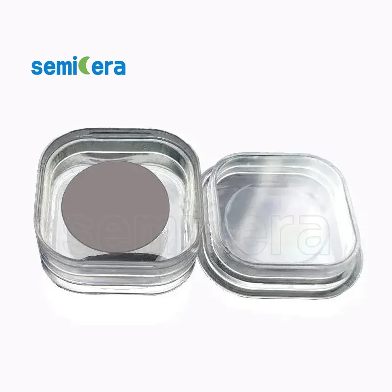
Semicera is proud to present the 30mm Aluminum Nitride Wafer Substrate, a top-tier material engineered to meet the stringent demands of modern electronic and optoelectronic applications. Aluminum Nitride (AlN) substrates are renowned for their outstanding thermal conductivity and electrical insulation properties, making them an ideal choice for high-performance devices.
Características clave:
• Exceptional Thermal Conductivity: El 30mm Aluminum Nitride Wafer Substrate boasts a thermal conductivity of up to 170 W/mK, significantly higher than other substrate materials, ensuring efficient heat dissipation in high-power applications.
• High Electrical Insulation: With excellent electrical insulating properties, this substrate minimizes cross-talk and signal interference, making it ideal for RF and microwave applications.
• Mechanical Strength: El 30mm Aluminum Nitride Wafer Substrate offers superior mechanical strength and stability, ensuring durability and reliability even under rigorous operating conditions.
• Versatile Applications: This substrate is perfect for use in high-power LEDs, laser diodes, and RF components, providing a robust and reliable foundation for your most demanding projects.
• Precision Fabrication: Semicera ensures that each wafer substrate is fabricated with the highest precision, offering uniform thickness and surface quality to meet the exacting standards of advanced electronic devices.
Maximize the efficiency and reliability of your devices with Semicera’s 30mm Aluminum Nitride Wafer Substrate. Our substrates are designed to deliver superior performance, ensuring that your electronic and optoelectronic systems operate at their best. Trust Semicera for cutting-edge materials that lead the industry in quality and innovation.
|
Elementos |
Producción |
Investigación |
Ficticio |
|
Parámetros de cristal |
|||
|
Politito |
4H |
||
|
Error de orientación de la superficie |
4±0.15° |
||
|
Parámetros eléctricos |
|||
|
Dopante |
nitrógeno de tipo N |
||
|
Resistividad |
0.015-0.025ohm · cm |
||
|
Parámetros mecánicos |
|||
|
Diámetro |
150.0 ± 0.2 mm |
||
|
Espesor |
350 ± 25 µm |
||
|
Orientación plana primaria |
[1-100]±5° |
||
|
Longitud plana primaria |
47.5 ± 1.5 mm |
||
|
Plano secundario |
Ninguno |
||
|
TTV |
≤5 µm |
≤10 µm |
≤15 µm |
|
LTV |
≤3 μm (5 mm*5 mm) |
≤5 μm (5 mm*5 mm) |
≤10 μm (5 mm*5 mm) |
|
Arco |
-15 μm ~ 15 μm |
-35 μm ~ 35 μm |
-45 μm ~ 45 μm |
|
Urdimbre |
≤35 µm |
≤45 µm |
≤55 µm |
|
Rugosidad delantera (SI-FACE) (AFM) |
RA≤0.2Nm (5 μm*5 μm) |
||
|
Estructura |
|||
|
Densidad de micropipe |
<1 ea/cm2 |
<10 ea/cm2 |
<15 ea/cm2 |
|
Impurezas de metal |
≤5E10atoms/cm2 |
N / A |
|
|
BPD |
≤1500 ea/cm2 |
≤3000 ea/cm2 |
N / A |
|
TSD |
≤500 ea/cm2 |
≤1000 ea/cm2 |
N / A |
|
Calidad frontal |
|||
|
Frente |
Si |
||
|
Acabado superficial |
SI-FACE CMP |
||
|
Partículas |
≤60ea/oblea (tamaño ≥0.3 μm) |
N / A |
|
|
Arañazos |
≤5ea/mm. Longitud acumulativa ≤diameter |
Longitud acumulativa ≤2*diámetro |
N / A |
|
Peel de naranja/pits/manchas/estrías/grietas/contaminación |
Ninguno |
N / A |
|
|
Chips de borde/sangría/placas hexagonales |
Ninguno |
||
|
Áreas de politype |
Ninguno |
Área acumulada ≤20% |
Área acumulada ≤30% |
|
Marcado láser delantero |
Ninguno |
||
|
Calidad espalda |
|||
|
Final |
CMP C-FACE |
||
|
Arañazos |
≤5EA/mm, longitud acumulativa ≤2*diámetro |
N / A |
|
|
Defectos posteriores (chips/muescas de borde) |
Ninguno |
||
|
Rugosidad |
RA≤0.2Nm (5 μm*5 μm) |
||
|
Marcado láser de espalda |
1 mm (desde el borde superior) |
||
|
Borde |
|||
|
Borde |
Chaflán |
||
|
Embalaje |
|||
|
Embalaje |
Lista de EPI con embalaje de vacío Embalaje de cassette de múltiples obras |
||
|
*Notas: "NA" significa que ningún elemento de solicitud no mencionado puede referirse a SEMI-STD. |
|||


