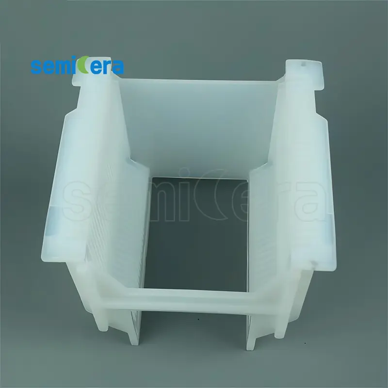
Semicera presents the industry-leading Transportista de obleas, engineered to provide superior protection and seamless transportation of delicate semiconductor wafers across various stages of the manufacturing process. Our Transportista de obleas are meticulously designed to meet the stringent demands of modern semiconductor fabrication, ensuring the integrity and quality of your wafers are maintained at all times.
Características clave:
• Premium Material Construction: Crafted from high-quality, contamination-resistant materials that guarantee durability and longevity, making them ideal for cleanroom environments.
• Precision Design: Features precise slot alignment and secure holding mechanisms to prevent wafer slippage and damage during handling and transportation.
• Versatile Compatibility: Accommodates a wide range of wafer sizes and thicknesses, providing flexibility for various semiconductor applications.
• Ergonomic Handling: Lightweight and user-friendly design facilitates easy loading and unloading, enhancing operational efficiency and reducing handling time.
• Customizable Options: Offers customization to meet specific requirements, including material choice, size adjustments, and labeling for optimized workflow integration.
Enhance your semiconductor manufacturing process with Semicera’s Transportista de obleas, the perfect solution for safeguarding your wafers against contamination and mechanical damage. Trust in our commitment to quality and innovation to deliver products that not only meet but exceed industry standards, ensuring your operations run smoothly and efficiently.
|
Elementos |
Producción |
Investigación |
Ficticio |
|
Parámetros de cristal |
|||
|
Politito |
4H |
||
|
Error de orientación de la superficie |
4±0.15° |
||
|
Parámetros eléctricos |
|||
|
Dopante |
nitrógeno de tipo N |
||
|
Resistividad |
0.015-0.025ohm · cm |
||
|
Parámetros mecánicos |
|||
|
Diámetro |
150.0 ± 0.2 mm |
||
|
Espesor |
350 ± 25 µm |
||
|
Orientación plana primaria |
[1-100]±5° |
||
|
Longitud plana primaria |
47.5 ± 1.5 mm |
||
|
Plano secundario |
Ninguno |
||
|
TTV |
≤5 µm |
≤10 µm |
≤15 µm |
|
LTV |
≤3 μm (5 mm*5 mm) |
≤5 μm (5 mm*5 mm) |
≤10 μm (5 mm*5 mm) |
|
Arco |
-15 μm ~ 15 μm |
-35 μm ~ 35 μm |
-45 μm ~ 45 μm |
|
Urdimbre |
≤35 µm |
≤45 µm |
≤55 µm |
|
Rugosidad delantera (SI-FACE) (AFM) |
RA≤0.2Nm (5 μm*5 μm) |
||
|
Estructura |
|||
|
Densidad de micropipe |
<1 ea/cm2 |
<10 ea/cm2 |
<15 ea/cm2 |
|
Impurezas de metal |
≤5E10atoms/cm2 |
N / A |
|
|
BPD |
≤1500 ea/cm2 |
≤3000 ea/cm2 |
N / A |
|
TSD |
≤500 ea/cm2 |
≤1000 ea/cm2 |
N / A |
|
Calidad frontal |
|||
|
Frente |
Si |
||
|
Acabado superficial |
SI-FACE CMP |
||
|
Partículas |
≤60ea/oblea (tamaño ≥0.3 μm) |
N / A |
|
|
Arañazos |
≤5ea/mm. Longitud acumulativa ≤diameter |
Longitud acumulativa ≤2*diámetro |
N / A |
|
Peel de naranja/pits/manchas/estrías/grietas/contaminación |
Ninguno |
N / A |
|
|
Chips de borde/sangría/placas hexagonales |
Ninguno |
||
|
Áreas de politype |
Ninguno |
Área acumulada ≤20% |
Área acumulada ≤30% |
|
Marcado láser delantero |
Ninguno |
||
|
Calidad espalda |
|||
|
Final |
CMP C-FACE |
||
|
Arañazos |
≤5EA/mm, longitud acumulativa ≤2*diámetro |
N / A |
|
|
Defectos posteriores (chips/muescas de borde) |
Ninguno |
||
|
Rugosidad |
RA≤0.2Nm (5 μm*5 μm) |
||
|
Marcado láser de espalda |
1 mm (desde el borde superior) |
||
|
Borde |
|||
|
Borde |
Chaflán |
||
|
Embalaje |
|||
|
Embalaje |
Lista de EPI con embalaje de vacío Embalaje de cassette de múltiples obras |
||
|
*Notas: "NA" significa que ningún elemento de solicitud no mencionado puede referirse a SEMI-STD. |
|||


