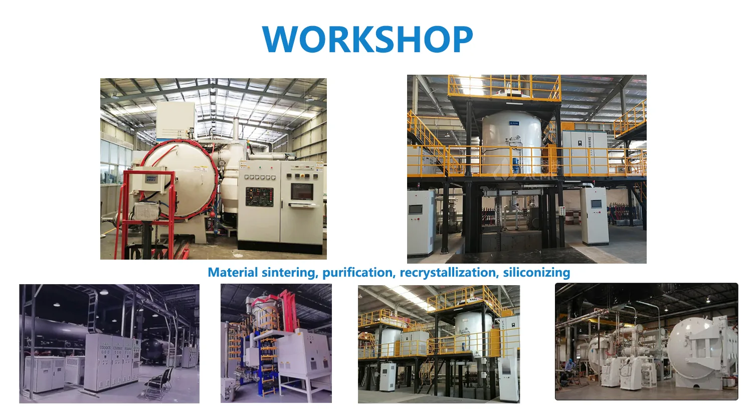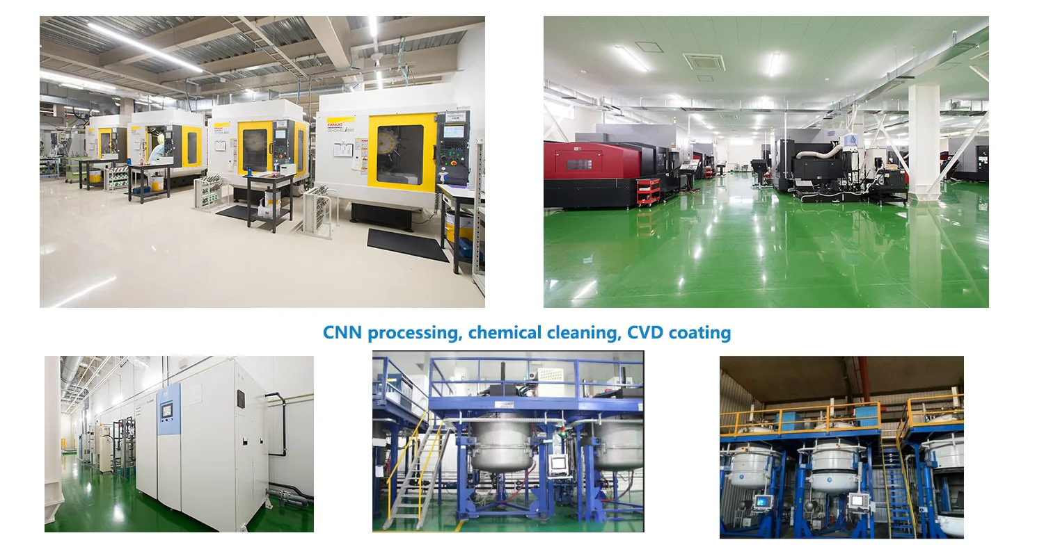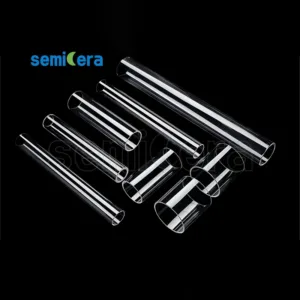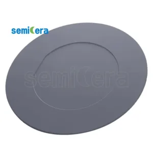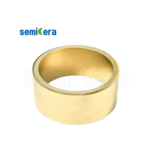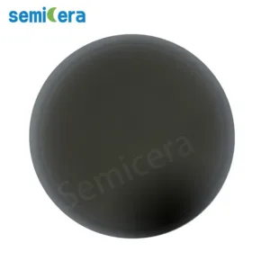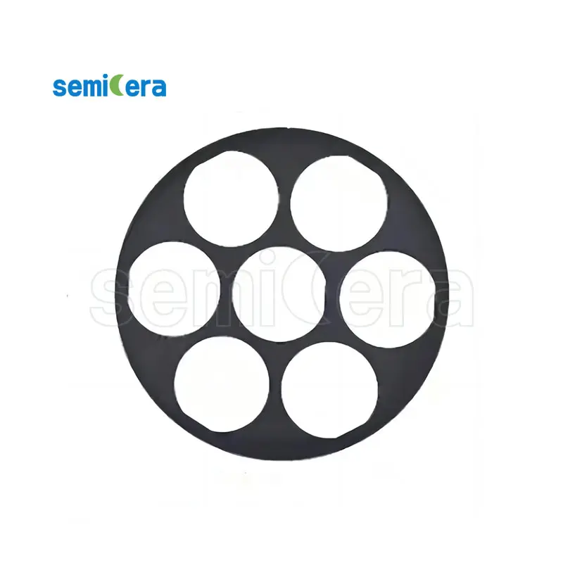
Descripción del Producto
Nuestra compañía proporciona servicios de procesos de recubrimiento SIC mediante el método de CVD en la superficie del grafito, la cerámica y otros materiales, de modo que los gases especiales que contienen carbono y silicio reaccionan a alta temperatura para obtener moléculas SiC de alta pureza, moléculas depositadas en la superficie de los materiales recubiertos, formando una capa protectora SIC.
Características principales:
1. Resistencia a la oxidación de alta temperatura:
La resistencia a la oxidación sigue siendo muy buena cuando la temperatura es tan alta como 1600 C.
2. Alta pureza: hecha por deposición de vapor químico en una condición de cloración de alta temperatura.
3. Resistencia a la erosión: alta dureza, superficie compacta, partículas finas.
4. Resistencia a la corrosión: ácido, álcali, sal y reactivos orgánicos.


Especificaciones principales de recubrimiento CVD-SIC
|
Propiedades de SIC-CVD |
||
|
Estructura cristalina |
Fase FCC β |
|
|
Densidad |
g/cm ³ |
3.21 |
|
Dureza |
Dureza de Vickers |
2500 |
|
Tamaño de grano |
mm |
2~10 |
|
Pureza química |
% |
99.99995 |
|
Capacidad de calor |
J · KG-1 · K-1 |
640 |
|
Temperatura de sublimación |
℃ |
2700 |
|
Fuerza del felexural |
MPA (RT 4 puntos) |
415 |
|
Módulo de Young |
GPA (4pt Bend, 1300 ℃) |
430 |
|
Expansión térmica (CTE) |
10-6K-1 |
4.5 |
|
Conductividad térmica |
(W/mk) |
300 |