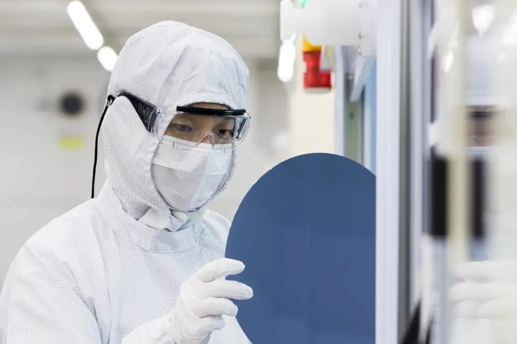
Silicon carbide (SiC) single crystal material has a large band gap width (~Si 3 times), high thermal conductivity (~Si 3.3 times or GaAs 10 times), high electron saturation migration rate (~Si 2.5 times), high breakdown electric field (~Si 10 times or GaAs 5 times) and other outstanding characteristics.
Semicera energy can provide customers with high-quality Conductive (Conductive), Semi-insulating (Semi-insulating), HPSI (High Purity semi-insulating) silicon carbide substrate; In addition, we can provide customers with homogeneous and heterogeneous silicon carbide epitaxial sheets; We can also customize the epitaxial sheet according to the specific needs of customers, and there is no minimum order quantity.
|
Elementos |
Producción |
Investigación |
Ficticio |
|
Parámetros de cristal |
|||
|
Politito |
4H |
||
|
Error de orientación de la superficie |
<11-20 >4±0.15° |
||
|
Parámetros eléctricos |
|||
|
Dopante |
nitrógeno de tipo N |
||
|
Resistividad |
0.015-0.025ohm·cm |
||
|
Parámetros mecánicos |
|||
|
Diámetro |
99.5 – 100mm |
||
|
Espesor |
350±25 μm |
||
|
Orientación plana primaria |
[1-100]±5° |
||
|
Longitud plana primaria |
32.5±1.5mm |
||
|
Secondary flat position |
90° CW from primary flat ±5°. silicon face up |
||
|
Secondary flat length |
18±1.5mm |
||
|
TTV |
≤5 μm |
≤10 μm |
≤20 μm |
|
LTV |
≤2 μm(5mm*5mm) |
≤5 μm(5mm*5mm) |
N / A |
|
Arco |
-15μm ~ 15μm |
-35μm ~ 35μm |
-45μm ~ 45μm |
|
Urdimbre |
≤20 μm |
≤45 μm |
≤50 μm |
|
Rugosidad delantera (SI-FACE) (AFM) |
Ra≤0.2nm (5μm*5μm) |
||
|
Estructura |
|||
|
Densidad de micropipe |
≤1 ea/cm2 |
≤5 ea/cm2 |
≤10 ea/cm2 |
|
Impurezas de metal |
≤5E10atoms/cm2 |
N / A |
|
|
BPD |
≤1500 ea/cm2 |
≤3000 ea/cm2 |
N / A |
|
TSD |
≤500 ea/cm2 |
≤1000 ea/cm2 |
N / A |
|
Calidad frontal |
|||
|
Frente |
Si |
||
|
Acabado superficial |
SI-FACE CMP |
||
|
Partículas |
≤60ea/wafer (size≥0.3μm) |
N / A |
|
|
Arañazos |
≤2ea/mm. Cumulative length ≤Diameter |
Cumulative length≤2*Diameter |
N / A |
|
Peel de naranja/pits/manchas/estrías/grietas/contaminación |
Ninguno |
N / A |
|
|
Chips de borde/sangría/placas hexagonales |
Ninguno |
N / A |
|
|
Áreas de politype |
Ninguno |
Cumulative area≤20% |
Cumulative area≤30% |
|
Marcado láser delantero |
Ninguno |
||
|
Calidad espalda |
|||
|
Final |
CMP C-FACE |
||
|
Arañazos |
≤5ea/mm,Cumulative length≤2*Diameter |
N / A |
|
|
Defectos posteriores (chips/muescas de borde) |
Ninguno |
||
|
Rugosidad |
Ra≤0.2nm (5μm*5μm) |
||
|
Marcado láser de espalda |
1 mm (desde el borde superior) |
||
|
Borde |
|||
|
Borde |
Chaflán |
||
|
Embalaje |
|||
|
Embalaje |
The inner bag is filled with nitrogen and the outer bag is vacuumed. Multi-wafer cassette, epi-ready. |
||
|
*Notas: "NA" significa que ningún elemento de solicitud no mencionado puede referirse a SEMI-STD. |
|||