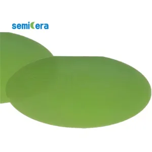
Semicera is excited to offer 2″ Gallium Oxide Substrates, a cutting-edge material designed to enhance the performance of advanced semiconductor devices. These substrates, made from Gallium Oxide (Ga2O3), feature an ultra-wide bandgap, making them an ideal choice for high-power, high-frequency, and UV optoelectronic applications.
Características clave:
• Ultra-Wide Bandgap: El 2″ Gallium Oxide Substrates provide an outstanding bandgap of approximately 4.8 eV, allowing for higher voltage and temperature operation, far exceeding the capabilities of traditional semiconductor materials like silicon.
• Exceptional Breakdown Voltage: These substrates enable devices to handle significantly higher voltages, making them perfect for power electronics, especially in high-voltage applications.
• Excellent Thermal Conductivity: With superior thermal stability, these substrates maintain consistent performance even in extreme thermal environments, ideal for high-power and high-temperature applications.
• High-Quality Material: El 2″ Gallium Oxide Substrates offer low defect densities and high crystalline quality, ensuring the reliable and efficient performance of your semiconductor devices.
• Versatile Applications: These substrates are suited for a range of applications, including power transistors, Schottky diodes, and UV-C LED devices, offering a robust foundation for both power and optoelectronic innovations.
Unlock the full potential of your semiconductor devices with Semicera’s 2″ Gallium Oxide Substrates. Our substrates are designed to meet the demanding needs of today’s advanced applications, ensuring high performance, reliability, and efficiency. Choose Semicera for state-of-the-art semiconductor materials that drive innovation.
|
Elementos |
Producción |
Investigación |
Ficticio |
|
Parámetros de cristal |
|||
|
Politito |
4H |
||
|
Error de orientación de la superficie |
4±0.15° |
||
|
Parámetros eléctricos |
|||
|
Dopante |
nitrógeno de tipo N |
||
|
Resistividad |
0.015-0.025ohm · cm |
||
|
Parámetros mecánicos |
|||
|
Diámetro |
150.0 ± 0.2 mm |
||
|
Espesor |
350 ± 25 µm |
||
|
Orientación plana primaria |
[1-100]±5° |
||
|
Longitud plana primaria |
47.5 ± 1.5 mm |
||
|
Plano secundario |
Ninguno |
||
|
TTV |
≤5 µm |
≤10 µm |
≤15 µm |
|
LTV |
≤3 μm (5 mm*5 mm) |
≤5 μm (5 mm*5 mm) |
≤10 μm (5 mm*5 mm) |
|
Arco |
-15 μm ~ 15 μm |
-35 μm ~ 35 μm |
-45 μm ~ 45 μm |
|
Urdimbre |
≤35 µm |
≤45 µm |
≤55 µm |
|
Rugosidad delantera (SI-FACE) (AFM) |
RA≤0.2Nm (5 μm*5 μm) |
||
|
Estructura |
|||
|
Densidad de micropipe |
<1 ea/cm2 |
<10 ea/cm2 |
<15 ea/cm2 |
|
Impurezas de metal |
≤5E10atoms/cm2 |
N / A |
|
|
BPD |
≤1500 ea/cm2 |
≤3000 ea/cm2 |
N / A |
|
TSD |
≤500 ea/cm2 |
≤1000 ea/cm2 |
N / A |
|
Calidad frontal |
|||
|
Frente |
Si |
||
|
Acabado superficial |
SI-FACE CMP |
||
|
Partículas |
≤60ea/oblea (tamaño ≥0.3 μm) |
N / A |
|
|
Arañazos |
≤5ea/mm. Longitud acumulativa ≤diameter |
Longitud acumulativa ≤2*diámetro |
N / A |
|
Peel de naranja/pits/manchas/estrías/grietas/contaminación |
Ninguno |
N / A |
|
|
Chips de borde/sangría/placas hexagonales |
Ninguno |
||
|
Áreas de politype |
Ninguno |
Área acumulada ≤20% |
Área acumulada ≤30% |
|
Marcado láser delantero |
Ninguno |
||
|
Calidad espalda |
|||
|
Final |
CMP C-FACE |
||
|
Arañazos |
≤5EA/mm, longitud acumulativa ≤2*diámetro |
N / A |
|
|
Defectos posteriores (chips/muescas de borde) |
Ninguno |
||
|
Rugosidad |
RA≤0.2Nm (5 μm*5 μm) |
||
|
Marcado láser de espalda |
1 mm (desde el borde superior) |
||
|
Borde |
|||
|
Borde |
Chaflán |
||
|
Embalaje |
|||
|
Embalaje |
Lista de EPI con embalaje de vacío Embalaje de cassette de múltiples obras |
||
|
*Notas: "NA" significa que ningún elemento de solicitud no mencionado puede referirse a SEMI-STD. |
|||