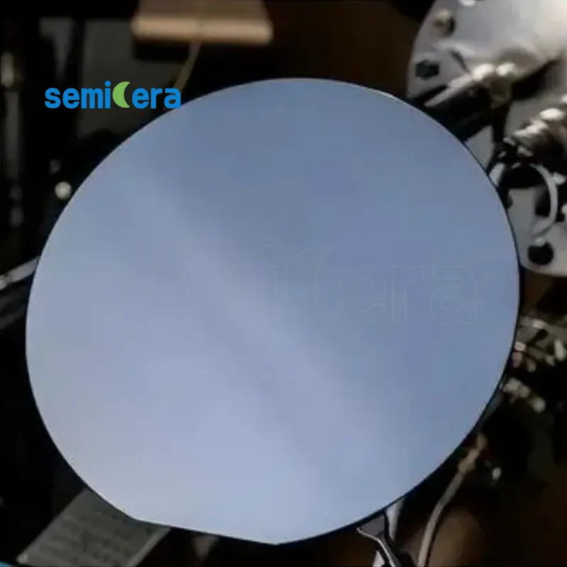
Semicera proudly offers Ga2O3 Epitaxy, a state-of-the-art solution designed to push the boundaries of power electronics and optoelectronics. This advanced epitaxial technology leverages the unique properties of Gallium Oxide (Ga2O3) to deliver superior performance in demanding applications.
Características clave:
• Exceptional Wide Bandgap: Ga2O3 Epitaxy features an ultra-wide bandgap, allowing for higher breakdown voltages and efficient operation in high-power environments.
• High Thermal Conductivity: The epitaxial layer provides excellent thermal conductivity, ensuring stable operation even under high-temperature conditions, making it ideal for high-frequency devices.
• Superior Material Quality: Achieve high crystal quality with minimal defects, ensuring optimal device performance and longevity, especially in critical applications such as power transistors and UV detectors.
• Versatility in Applications: Perfectly suited for power electronics, RF applications, and optoelectronics, providing a reliable foundation for next-generation semiconductor devices.
Discover the potential of Ga2O3 Epitaxy with Semicera’s innovative solutions. Our epitaxial products are designed to meet the highest standards of quality and performance, enabling your devices to operate with maximum efficiency and reliability. Choose Semicera for cutting-edge semiconductor technology.
|
Elementos |
Producción |
Investigación |
Ficticio |
|
Parámetros de cristal |
|||
|
Politito |
4H |
||
|
Error de orientación de la superficie |
4±0.15° |
||
|
Parámetros eléctricos |
|||
|
Dopante |
nitrógeno de tipo N |
||
|
Resistividad |
0.015-0.025ohm · cm |
||
|
Parámetros mecánicos |
|||
|
Diámetro |
150.0 ± 0.2 mm |
||
|
Espesor |
350 ± 25 µm |
||
|
Orientación plana primaria |
[1-100]±5° |
||
|
Longitud plana primaria |
47.5 ± 1.5 mm |
||
|
Plano secundario |
Ninguno |
||
|
TTV |
≤5 µm |
≤10 µm |
≤15 µm |
|
LTV |
≤3 μm (5 mm*5 mm) |
≤5 μm (5 mm*5 mm) |
≤10 μm (5 mm*5 mm) |
|
Arco |
-15 μm ~ 15 μm |
-35 μm ~ 35 μm |
-45 μm ~ 45 μm |
|
Urdimbre |
≤35 µm |
≤45 µm |
≤55 µm |
|
Rugosidad delantera (SI-FACE) (AFM) |
RA≤0.2Nm (5 μm*5 μm) |
||
|
Estructura |
|||
|
Densidad de micropipe |
<1 ea/cm2 |
<10 ea/cm2 |
<15 ea/cm2 |
|
Impurezas de metal |
≤5E10atoms/cm2 |
N / A |
|
|
BPD |
≤1500 ea/cm2 |
≤3000 ea/cm2 |
N / A |
|
TSD |
≤500 ea/cm2 |
≤1000 ea/cm2 |
N / A |
|
Calidad frontal |
|||
|
Frente |
Si |
||
|
Acabado superficial |
SI-FACE CMP |
||
|
Partículas |
≤60ea/oblea (tamaño ≥0.3 μm) |
N / A |
|
|
Arañazos |
≤5ea/mm. Longitud acumulativa ≤diameter |
Longitud acumulativa ≤2*diámetro |
N / A |
|
Peel de naranja/pits/manchas/estrías/grietas/contaminación |
Ninguno |
N / A |
|
|
Chips de borde/sangría/placas hexagonales |
Ninguno |
||
|
Áreas de politype |
Ninguno |
Área acumulada ≤20% |
Área acumulada ≤30% |
|
Marcado láser delantero |
Ninguno |
||
|
Calidad espalda |
|||
|
Final |
CMP C-FACE |
||
|
Arañazos |
≤5EA/mm, longitud acumulativa ≤2*diámetro |
N / A |
|
|
Defectos posteriores (chips/muescas de borde) |
Ninguno |
||
|
Rugosidad |
RA≤0.2Nm (5 μm*5 μm) |
||
|
Marcado láser de espalda |
1 mm (desde el borde superior) |
||
|
Borde |
|||
|
Borde |
Chaflán |
||
|
Embalaje |
|||
|
Embalaje |
Lista de EPI con embalaje de vacío Embalaje de cassette de múltiples obras |
||
|
*Notas: "NA" significa que ningún elemento de solicitud no mencionado puede referirse a SEMI-STD. |
|||


