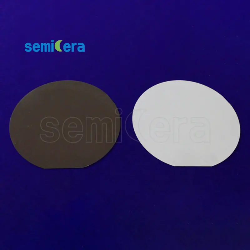
Semicera’s LiNbO3 Bonding Wafer is designed to meet the high demands of advanced semiconductor manufacturing. With its exceptional properties, including superior wear resistance, high thermal stability, and outstanding purity, this wafer is ideal for use in applications that require precision and long-lasting performance.
In the semiconductor industry, LiNbO3 Bonding Wafers are commonly used for bonding thin layers in optoelectronic devices, sensors, and advanced ICs. They are particularly valued in photonics and MEMS (Micro-Electromechanical Systems) due to their excellent dielectric properties and ability to withstand harsh operating conditions. Semicera’s LiNbO3 Bonding Wafer is engineered to support precise layer bonding, enhancing the overall performance and reliability of semiconductor devices.
| Propiedades térmicas y eléctricas de Linbo3 | |
| Punto de fusión | 1250 ℃ |
| Temperatura curie | 1140 ℃ |
| Conductividad térmica | 38 w/m/k @ 25 ℃ |
| Coeficiente de expansión térmica (@ 25 ° C) |
//a , 2.0 × 10⁻⁶ /K //c , 2.2 × 10⁻⁶ /K |
| Resistividad | 2 × 10⁻⁶ Ω · cm @ 200 ℃ |
| Constante dieléctrica |
ES11/E0 = 43 , ET11/E0 = 78 ES33/E0 = 28 , ET33/E0 = 2 |
| Constante piezoeléctrica |
D22=2.04 × 10⁻¹¹ C/n D33=19.22 × 10⁻¹¹ C/n |
| Coeficiente electroóptico |
Connecticut33=32 PM/V , γs33=31 pm/v , Connecticut31=10 PM/V , γs31=8.6 pm/v , Connecticut22=6.8 PM/V , γs22=3.4 pm/v , |
|
Voltaje de media onda, DC |
3.03 kV 4.02 kV |
Crafted using top-quality materials, the LiNbO3 Bonding Wafer ensures consistent reliability even under extreme conditions. Its high thermal stability makes it particularly suitable for environments involving elevated temperatures, such as those found in semiconductor epitaxy processes. Additionally, the wafer’s high purity ensures minimal contamination, making it a trusted choice for critical semiconductor applications.
At Semicera, we are committed to providing industry-leading solutions. Our LiNbO3 Bonding Wafer delivers unmatched durability and high-performance capabilities for applications requiring high purity, wear resistance, and thermal stability. Whether for advanced semiconductor production or other specialized technologies, this wafer serves as an essential component for cutting-edge device manufacturing.