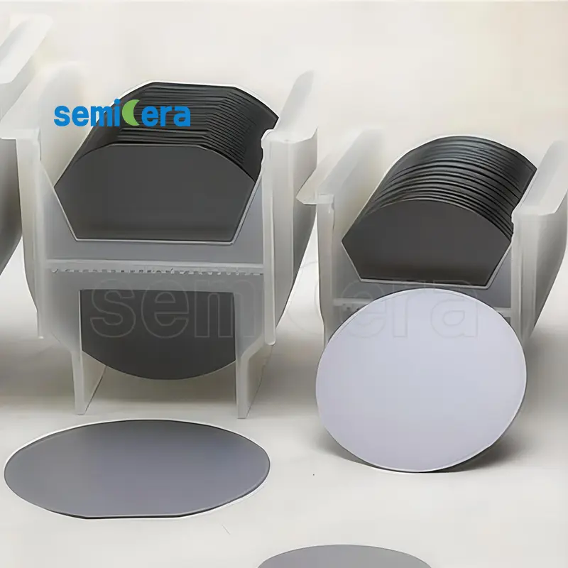
Semicera Silicon Wafers are meticulously crafted to serve as the foundation for a wide array of semiconductor devices, from microprocessors to photovoltaic cells. These wafers are engineered with high precision and purity, ensuring optimal performance in various electronic applications.
Manufactured using advanced techniques, Semicera Silicon Wafers exhibit exceptional flatness and uniformity, which are crucial for achieving high yields in semiconductor fabrication. This level of precision helps in minimizing defects and improving the overall efficiency of electronic components.
The superior quality of Semicera Silicon Wafers is evident in their electrical characteristics, which contribute to the enhanced performance of semiconductor devices. With low impurity levels and high crystal quality, these wafers provide the ideal platform for developing high-performance electronics.
Available in various sizes and specifications, Semicera Silicon Wafers can be tailored to meet the specific needs of different industries, including computing, telecommunications, and renewable energy. Whether for large-scale manufacturing or specialized research, these wafers deliver reliable results.
Semicera is committed to supporting the growth and innovation of the semiconductor industry by providing high-quality silicon wafers that meet the highest industry standards. With a focus on precision and reliability, Semicera enables manufacturers to push the boundaries of technology, ensuring their products stay at the forefront of the market.
|
Elementos |
Producción |
Investigación |
Ficticio |
|
Parámetros de cristal |
|||
|
Politito |
4H |
||
|
Error de orientación de la superficie |
4±0.15° |
||
|
Parámetros eléctricos |
|||
|
Dopante |
nitrógeno de tipo N |
||
|
Resistividad |
0.015-0.025ohm · cm |
||
|
Parámetros mecánicos |
|||
|
Diámetro |
150.0 ± 0.2 mm |
||
|
Espesor |
350 ± 25 µm |
||
|
Orientación plana primaria |
[1-100]±5° |
||
|
Longitud plana primaria |
47.5 ± 1.5 mm |
||
|
Plano secundario |
Ninguno |
||
|
TTV |
≤5 µm |
≤10 µm |
≤15 µm |
|
LTV |
≤3 μm (5 mm*5 mm) |
≤5 μm (5 mm*5 mm) |
≤10 μm (5 mm*5 mm) |
|
Arco |
-15 μm ~ 15 μm |
-35 μm ~ 35 μm |
-45 μm ~ 45 μm |
|
Urdimbre |
≤35 µm |
≤45 µm |
≤55 µm |
|
Rugosidad delantera (SI-FACE) (AFM) |
RA≤0.2Nm (5 μm*5 μm) |
||
|
Estructura |
|||
|
Densidad de micropipe |
<1 ea/cm2 |
<10 ea/cm2 |
<15 ea/cm2 |
|
Impurezas de metal |
≤5E10atoms/cm2 |
N / A |
|
|
BPD |
≤1500 ea/cm2 |
≤3000 ea/cm2 |
N / A |
|
TSD |
≤500 ea/cm2 |
≤1000 ea/cm2 |
N / A |
|
Calidad frontal |
|||
|
Frente |
Si |
||
|
Acabado superficial |
SI-FACE CMP |
||
|
Partículas |
≤60ea/oblea (tamaño ≥0.3 μm) |
N / A |
|
|
Arañazos |
≤5ea/mm. Longitud acumulativa ≤diameter |
Longitud acumulativa ≤2*diámetro |
N / A |
|
Peel de naranja/pits/manchas/estrías/grietas/contaminación |
Ninguno |
N / A |
|
|
Chips de borde/sangría/placas hexagonales |
Ninguno |
||
|
Áreas de politype |
Ninguno |
Área acumulada ≤20% |
Área acumulada ≤30% |
|
Marcado láser delantero |
Ninguno |
||
|
Calidad espalda |
|||
|
Final |
CMP C-FACE |
||
|
Arañazos |
≤5EA/mm, longitud acumulativa ≤2*diámetro |
N / A |
|
|
Defectos posteriores (chips/muescas de borde) |
Ninguno |
||
|
Rugosidad |
RA≤0.2Nm (5 μm*5 μm) |
||
|
Marcado láser de espalda |
1 mm (desde el borde superior) |
||
|
Borde |
|||
|
Borde |
Chaflán |
||
|
Embalaje |
|||
|
Embalaje |
Lista de EPI con embalaje de vacío Embalaje de cassette de múltiples obras |
||
|
*Notas: "NA" significa que ningún elemento de solicitud no mencionado puede referirse a SEMI-STD. |
|||


