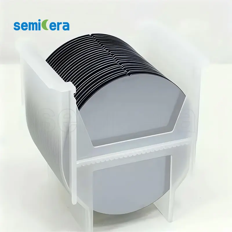
Semicera introduces the Wafer Cassette Carrier, a critical solution for the secure and efficient handling of semiconductor wafers. This carrier is engineered to meet the stringent requirements of the semiconductor industry, ensuring the protection and integrity of your wafers throughout the manufacturing process.
Características clave:
• Robust Construction: The Wafer Cassette Carrier is built from high-quality, durable materials that withstand the rigors of semiconductor environments, providing reliable protection against contamination and physical damage.
• Precise Alignment: Designed for precise wafer alignment, this carrier ensures that wafers are securely held in place, minimizing the risk of misalignment or damage during transport.
• Easy Handling: Ergonomically designed for ease of use, the carrier simplifies the loading and unloading process, improving workflow efficiency in cleanroom environments.
• Compatibility: Compatible with a wide range of wafer sizes and types, making it versatile for various semiconductor manufacturing needs.
Experience unparalleled protection and convenience with Semicera’s Wafer Cassette Carrier. Our carrier is designed to meet the highest standards of semiconductor manufacturing, ensuring your wafers remain in pristine condition from start to finish. Trust Semicera to deliver the quality and reliability you need for your most critical processes.
|
Elementos |
Producción |
Investigación |
Ficticio |
|
Parámetros de cristal |
|||
|
Politito |
4H |
||
|
Error de orientación de la superficie |
4±0.15° |
||
|
Parámetros eléctricos |
|||
|
Dopante |
nitrógeno de tipo N |
||
|
Resistividad |
0.015-0.025ohm · cm |
||
|
Parámetros mecánicos |
|||
|
Diámetro |
150.0 ± 0.2 mm |
||
|
Espesor |
350 ± 25 µm |
||
|
Orientación plana primaria |
[1-100]±5° |
||
|
Longitud plana primaria |
47.5 ± 1.5 mm |
||
|
Plano secundario |
Ninguno |
||
|
TTV |
≤5 µm |
≤10 µm |
≤15 µm |
|
LTV |
≤3 μm (5 mm*5 mm) |
≤5 μm (5 mm*5 mm) |
≤10 μm (5 mm*5 mm) |
|
Arco |
-15 μm ~ 15 μm |
-35 μm ~ 35 μm |
-45 μm ~ 45 μm |
|
Urdimbre |
≤35 µm |
≤45 µm |
≤55 µm |
|
Rugosidad delantera (SI-FACE) (AFM) |
RA≤0.2Nm (5 μm*5 μm) |
||
|
Estructura |
|||
|
Densidad de micropipe |
<1 ea/cm2 |
<10 ea/cm2 |
<15 ea/cm2 |
|
Impurezas de metal |
≤5E10atoms/cm2 |
N / A |
|
|
BPD |
≤1500 ea/cm2 |
≤3000 ea/cm2 |
N / A |
|
TSD |
≤500 ea/cm2 |
≤1000 ea/cm2 |
N / A |
|
Calidad frontal |
|||
|
Frente |
Si |
||
|
Acabado superficial |
SI-FACE CMP |
||
|
Partículas |
≤60ea/oblea (tamaño ≥0.3 μm) |
N / A |
|
|
Arañazos |
≤5ea/mm. Longitud acumulativa ≤diameter |
Longitud acumulativa ≤2*diámetro |
N / A |
|
Peel de naranja/pits/manchas/estrías/grietas/contaminación |
Ninguno |
N / A |
|
|
Chips de borde/sangría/placas hexagonales |
Ninguno |
||
|
Áreas de politype |
Ninguno |
Área acumulada ≤20% |
Área acumulada ≤30% |
|
Marcado láser delantero |
Ninguno |
||
|
Calidad espalda |
|||
|
Final |
CMP C-FACE |
||
|
Arañazos |
≤5EA/mm, longitud acumulativa ≤2*diámetro |
N / A |
|
|
Defectos posteriores (chips/muescas de borde) |
Ninguno |
||
|
Rugosidad |
RA≤0.2Nm (5 μm*5 μm) |
||
|
Marcado láser de espalda |
1 mm (desde el borde superior) |
||
|
Borde |
|||
|
Borde |
Chaflán |
||
|
Embalaje |
|||
|
Embalaje |
Lista de EPI con embalaje de vacío Embalaje de cassette de múltiples obras |
||
|
*Notas: "NA" significa que ningún elemento de solicitud no mencionado puede referirse a SEMI-STD. |
|||


