
The Real Reason Epitaxy Reactors Use SiC-Coated Heaters Instead of Bare Graphite
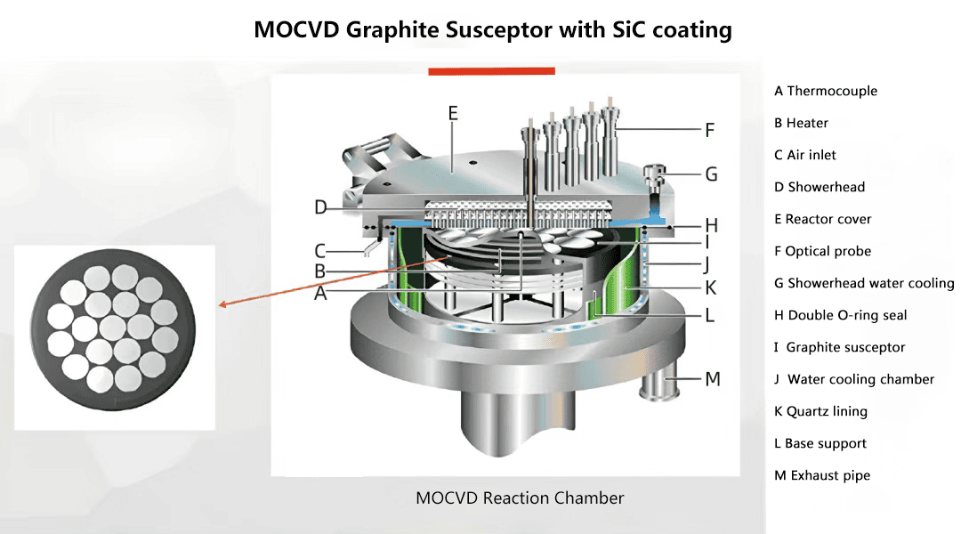
If you’ve ever opened up a CVD epitaxy reactor — whether it’s growing silicon epitaxial layers for power MOSFETs, 4H-SiC epitaxy for EV inverters, or GaN-on-SiC for RF devices — you’ll almost never find a heater or susceptor made of bare graphite sitting in the process zone. Instead, you’ll find graphite that has been coated with a dense layer of chemical-vapor-deposited silicon carbide (CVD-SiC), usually somewhere between 50 and 150 microns thick.
At first glance this seems like an odd extra step. Graphite is cheap, easy to machine, has excellent thermal shock resistance, and can be heated to over 2000°C without melting. So why do reactor OEMs and fabs insist on paying a premium for SiC-coated parts instead of just using bare graphite? The answer isn’t really about temperature at all — it’s about purity, chemistry, and particles, and understanding why requires looking at what actually happens to graphite inside a real epitaxy process.
1. Bare Graphite Was Never a “Clean” Material to Begin With
Graphite looks solid, but at the microstructural level it’s nothing like a dense ceramic. Commercial isostatic graphite is porous — typically 10-20% open porosity — with an interconnected network of pores that run through the bulk of the part. That porosity is actually useful for machining and thermal shock resistance, but it creates two serious problems in a semiconductor process chamber:
• Trapped impurities. Graphite is manufactured from petroleum coke or pitch precursors and almost always retains trace levels of boron, iron, vanadium, and other transition metals from the raw feedstock and furnacing process. Boron is the worst offender: it’s a p-type dopant in silicon, and even parts-per-million level boron in a graphite susceptor is enough to cause unintentional background doping in an epitaxial layer that’s supposed to be intrinsic or lightly doped.
• Outgassing under vacuum and heat. Because the pore network connects to the surface, adsorbed gases, moisture, and volatile impurities baked into the graphite during manufacturing slowly diffuse out once the part is heated to process temperature. This outgassing doesn’t stop after the first few runs — it continues for the life of the part, just at a declining rate, which makes it a persistent low-level contamination source rather than a one-time bake-out problem.
In other words, even a graphite susceptor with 99.999% (5N) bulk purity can still be a meaningful contamination source, because the exposed surface area inside those pores is enormous compared to the geometric surface area of the part.
2. The Bigger Problem: Graphite Reacts With the Process Gases
Epitaxy reactors don’t run in inert atmospheres. Depending on the process:
• Silicon epitaxy uses precursors like trichlorosilane (TCS), dichlorosilane (DCS), or silane, almost always with HCl either as an in-situ etch step or as a byproduct/carrier gas addition to suppress unwanted nucleation.
• SiC epitaxy runs at 1550-1650°C using silane and propane (or similar) precursors, again with HCl or chlorinated precursors increasingly common in modern “chlorine-based” SiC epitaxy chemistries to boost growth rate.
• GaN epitaxy on SiC or sapphire uses ammonia and metalorganic precursors like TMGa, and the hydrogen-rich, high-temperature ambient is also aggressive toward exposed carbon surfaces.
Bare graphite exposed to HCl, chlorine radicals, or even just hydrogen at high temperature is not chemically inert — it can be etched, and at epitaxy temperatures (1000°C and up), graphite is also susceptible to slow oxidation whenever trace oxygen or moisture is present. Every one of these reactions does two things at once:
• It generates particles. As graphite is etched or oxidized unevenly (grain boundaries and binder-rich regions erode faster than the bulk), it sheds carbon particulates directly into the gas stream flowing over the wafer. In an epitaxy process, particles landing on the wafer surface before or during growth become stacking faults, spikes, or point defects in the epitaxial layer — killer defects for power device and RF device yield.
• It slowly consumes the heater/susceptor itself. Each process cycle removes a small amount of material from the exposed graphite surface. Over hundreds of runs, this changes the part’s geometry, its thermal mass, and its emissivity — degrading temperature uniformity across the wafer and shortening the usable lifetime of an expensive precision-machined component.
This is really the core of the issue: bare graphite is not chemically compatible with the process gases used in epitaxy, and the consequence isn’t a dramatic failure — it’s a slow, insidious increase in particle counts and dopant contamination that shows up as yield loss long before anyone notices the heater itself degrading.
3. What a CVD-SiC Coating Actually Solves
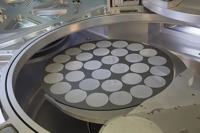
A CVD-SiC coating is grown directly onto the machined graphite part (typically via a methyltrichlorosilane, or MTS, CVD process at high temperature) to form a dense, adherent, essentially pore-free layer of polycrystalline silicon carbide over the graphite substrate. This single layer addresses every problem above simultaneously:
• Chemical inertness. Silicon carbide is vastly more resistant to attack by HCl, chlorine radicals, and hydrogen at epitaxy temperatures than graphite is. It’s also far more oxidation-resistant — SiC forms a thin, self-limiting, protective SiO2 layer when it does oxidize, rather than being consumed the way graphite is.
• A physical diffusion barrier. Because the coating is dense and (ideally) pinhole-free, it seals off the porous graphite substrate from the process atmosphere. Impurities trapped in the graphite bulk can no longer outgas into the chamber, and process gases can no longer penetrate into the graphite’s pore network to etch it from the inside out.
• Dramatically lower particle generation. SiC is a hard, chemically stable ceramic under these conditions, so the coated surface simply doesn’t shed material the way bare graphite does. This is the single biggest driver for using SiC-coated parts in modern epitaxy tools — particle performance is often the make-or-break spec for a susceptor or heater in a production fab.
• High-purity, high-emissivity thermal behavior. CVD-SiC can be produced at very high purity (often quoted at 5N-6N, i.e., 99.999-99.9999%), and its emissivity is both higher and more stable over time than oxidizing or eroding bare graphite. Since epitaxy reactors rely on radiative heating and precise temperature uniformity across the wafer (uniformity directly controls epi thickness and resistivity uniformity), a stable, well-characterized emissivity is a real process advantage, not just a purity nicety.
• Longer usable part life. Because the SiC coating protects the graphite from being etched away run after run, a coated heater or susceptor holds its dimensional tolerances and thermal characteristics far longer than an uncoated one — which matters a lot given how expensive and long-lead-time these precision graphite components typically are.
4. Why Not Just Use Solid SiC Instead of Coating Graphite?
This is the natural follow-up question, and the answer comes down to practicality. Bulk, fully-dense SiC is extremely hard and brittle, difficult and expensive to machine into the complex geometries that heaters and susceptors require (pockets for wafers, gas distribution channels, mounting features), and prone to cracking under the thermal cycling that a production reactor sees every single run.
Graphite, by contrast, machines easily into complex precision shapes and tolerates rapid heating and cooling extremely well because of its high thermal shock resistance. The SiC-coated graphite approach is really the best of both worlds: graphite provides the machinability, thermal shock tolerance, and mechanical robustness of the bulk part, while the thin CVD-SiC skin provides the chemical inertness, purity, and particle performance that the process actually requires at the exposed surface. You get graphite’s mechanical and thermal properties with silicon carbide’s surface chemistry — without paying the cost and yield penalty of machining brittle, expensive bulk SiC into complex shapes.
5. What This Means in Practice
For a fab or reactor engineer, the choice of SiC-coated versus bare graphite parts isn’t a minor BOM decision — it directly affects:
• Epi-layer purity, particularly background boron doping in silicon epitaxy, where even trace contamination shifts resistivity out of spec.
• Particle counts on the wafer, which map directly to defect density and device yield, especially for high-value power and RF devices.
• Preventive maintenance intervals, since a well-made SiC coating substantially extends the number of runs before a heater or susceptor needs to be reconditioned or replaced.
• Temperature uniformity drift over time, since a stable, unreactive surface keeps emissivity — and therefore radiative heating behavior — consistent from the first run to the last.
None of this is really about surviving high temperature; bare graphite can handle epitaxy temperatures just fine on its own. It’s about surviving repeated exposure to a chemically aggressive process atmosphere without shedding particles or leaching impurities into a layer that, in many cases, needs to be controlled down to parts-per-billion doping levels. That’s the real reason SiC-coated heaters replaced bare graphite as the default choice in modern epitaxy reactors — not exotic thermal performance, but the much more mundane, and much more important, demands of chemical inertness and cleanliness.