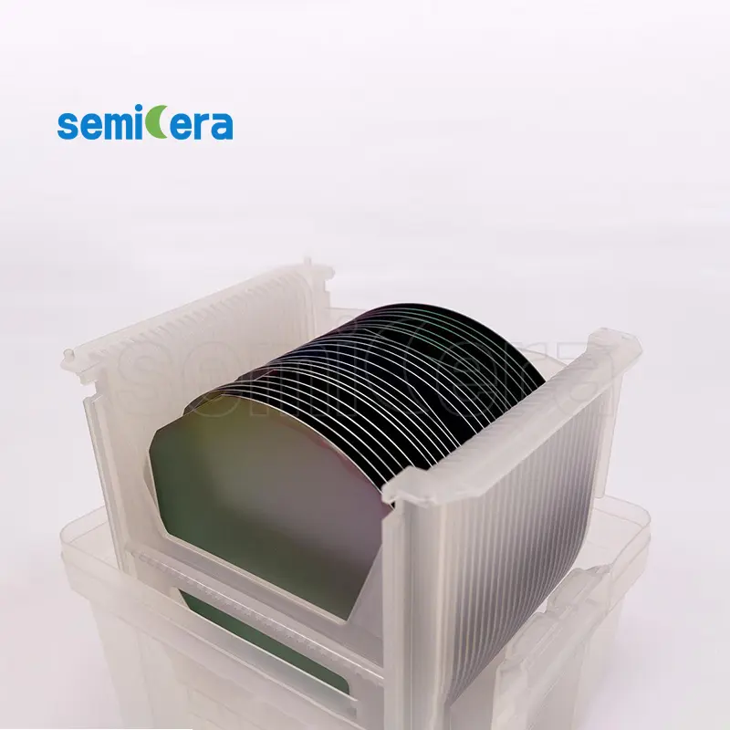
Seminer introduces the Cassette de semi-conducteurs, an essential tool for the secure and efficient handling of wafers throughout the semiconductor manufacturing process. Engineered with high precision, this cassette ensures that your wafers are safely stored and transported, maintaining their integrity at every stage.
Superior Protection and Durability Le Cassette de semi-conducteurs from Semicera is built to offer maximum protection to your wafers. Constructed from robust, contamination-resistant materials, it shields your wafers from potential damage and contamination, making it an ideal choice for cleanroom environments. The cassette’s design minimizes particulate generation and ensures that wafers remain untouched and secure during handling and transportation.
Enhanced Design for Optimal Performance Semicera’s Cassette de semi-conducteurs features a meticulously engineered design that provides precise wafer alignment, reducing the risk of misalignment and mechanical damage. The cassette’s slots are perfectly spaced to hold each wafer securely, preventing any movement that could result in scratches or other imperfections.
Versatility and Compatibility Le Cassette de semi-conducteurs is versatile and compatible with various wafer sizes, making it suitable for different stages of semiconductor fabrication. Whether you’re working with standard or custom wafer dimensions, this cassette adapts to your needs, offering flexibility in your manufacturing processes.
Streamlined Handling and Efficiency Designed with the user in mind, the Semicera Semiconductor Cassette is lightweight and easy to handle, allowing for quick and efficient loading and unloading. This ergonomic design not only saves time but also reduces the risk of human error, ensuring smooth operations within your facility.
Meeting Industry Standards Semicera ensures that the Cassette de semi-conducteurs meets the highest industry standards for quality and reliability. Each cassette undergoes rigorous testing to guarantee that it performs consistently under the demanding conditions of semiconductor manufacturing. This dedication to quality ensures that your wafers are always protected, maintaining the high standards required in the industry.
|
Articles |
Production |
Recherche |
Factice |
|
Paramètres de cristal |
|||
|
Polytype |
4H |
||
|
Erreur d'orientation de la surface |
4±0.15° |
||
|
Paramètres électriques |
|||
|
Dopant |
azote de type N |
||
|
Résistivité |
0,015-0.025ohm · cm |
||
|
Paramètres mécaniques |
|||
|
Diamètre |
150,0 ± 0,2 mm |
||
|
Épaisseur |
350 ± 25 µm |
||
|
Orientation plate primaire |
[1-100]±5° |
||
|
Longueur plate primaire |
47,5 ± 1,5 mm |
||
|
Plat secondaire |
Aucun |
||
|
TTV |
≤5 µm |
≤10 µm |
≤15 µm |
|
LTV |
≤3 μm (5 mm * 5 mm) |
≤5 μm (5 mm * 5 mm) |
≤10 μm (5 mm * 5 mm) |
|
Arc |
-15 μm ~ 15μm |
-35 μm ~ 35 μm |
-45 μm ~ 45 μm |
|
Chaîne |
≤35 µm |
≤45 µm |
≤55 µm |
|
Rugosité avant (si-face) (AFM) |
Ra≤0,2 nm (5 μm * 5 μm) |
||
|
Structure |
|||
|
Densité de micro- |
<1 ea / cm2 |
<10 ea / cm2 |
<15 ea / cm2 |
|
Impuretés métalliques |
≤5E10atoms/cm2 |
N / A |
|
|
BPB |
≤1500 ea / cm2 |
≤3000 ea / cm2 |
N / A |
|
TSD |
≤500 ea / cm2 |
≤1000 ea / cm2 |
N / A |
|
Qualité avant |
|||
|
Devant |
Si |
||
|
Finition de surface |
CMP SI-FACE |
||
|
Particules |
≤60ea / plaquette (taille 0,3 μm) |
N / A |
|
|
Rayures |
≤5EA / MM. Longueur cumulative ≤ diamètre |
Longueur cumulatif ≤2 * diamètre |
N / A |
|
PELLE / PEPES ORANGE / TAPPES / COMMENTS / CRESCHES / CONTAMINATION |
Aucun |
N / A |
|
|
Coups de bord / retraits / fracture / plaques hexagonales |
Aucun |
||
|
Zones de polytype |
Aucun |
Zone cumulative≤20% |
Zone cumulative ≤ 30% |
|
Marquage laser avant |
Aucun |
||
|
Qualité du dos |
|||
|
Finition arrière |
CMP C-FACE |
||
|
Rayures |
≤5ea / mm, longueur cumulative≤2 * diamètre |
N / A |
|
|
Défauts arrière (puces de bord / retraits) |
Aucun |
||
|
Rugosité du dos |
Ra≤0,2 nm (5 μm * 5 μm) |
||
|
Marquage laser arrière |
1 mm (du bord supérieur) |
||
|
Bord |
|||
|
Bord |
Chanfreiner |
||
|
Conditionnement |
|||
|
Conditionnement |
Préparé en épi avec un emballage sous vide Emballage de cassette multi-wafer |
||
|
*Remarques: «NA» signifie qu'aucun élément de demande non mentionné ne peut se référer au semi-std. |
|||


