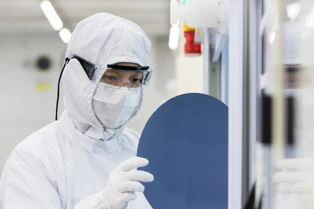
Semicera offers a wide range of 4H-8H SiC wafers. For many years, we have been a manufacturer and supplier of products to the semiconductor and photovoltaic industries. Our main products include: Silicon carbide etch plates, silicon carbide boat trailers, silicon carbide wafer boats (PV & Semiconductor), silicon carbide furnace tubes, silicon carbide cantilever paddles, silicon carbide chucks, silicon carbide beams, as well as CVD SiC coatings and TaC coatings. Covering most European and American markets. We look forward to being your long-term partner in China.
Silicon carbide (SiC) single crystal material has a large band gap width (~Si 3 times), high thermal conductivity (~Si 3.3 times or GaAs 10 times), high electron saturation migration rate (~Si 2.5 times), high breakdown electric field (~Si 10 times or GaAs 5 times) and other outstanding characteristics.
The third generation semiconductor materials mainly include SiC, GaN, diamond, etc., because its band gap width (Eg) is greater than or equal to 2.3 electron volts (eV), also known as wide band gap semiconductor materials. Compared with the first and second generation semiconductor materials, the third generation semiconductor materials have the advantages of high thermal conductivity, high breakdown electric field, high saturated electron migration rate and high bonding energy, which can meet the new requirements of modern electronic technology for high temperature, high power, high pressure, high frequency and radiation resistance and other harsh conditions. It has important application prospects in the fields of national defense, aviation, aerospace, oil exploration, optical storage, etc., and can reduce energy loss by more than 50% in many strategic industries such as broadband communications, solar energy, automobile manufacturing, semiconductor lighting, and smart grid, and can reduce equipment volume by more than 75%, which is of milestone significance for the development of human science and technology.
Semicera energy can provide customers with high-quality Conductive (Conductive), Semi-insulating (Semi-insulating), HPSI (High Purity semi-insulating) silicon carbide substrate; In addition, we can provide customers with homogeneous and heterogeneous silicon carbide epitaxial sheets; We can also customize the epitaxial sheet according to the specific needs of customers, and there is no minimum order quantity.
|
Articles |
Production |
Recherche |
Factice |
|
Paramètres de cristal |
|||
|
Polytype |
4H |
||
|
Erreur d'orientation de la surface |
<11-20 >4±0.15° |
||
|
Paramètres électriques |
|||
|
Dopant |
azote de type N |
||
|
Résistivité |
0.015-0.025ohm·cm |
||
|
Paramètres mécaniques |
|||
|
Diamètre |
150.0±0.2mm |
||
|
Épaisseur |
350±25 μm |
||
|
Orientation plate primaire |
[1-100]±5° |
||
|
Longueur plate primaire |
47.5±1.5mm |
||
|
Plat secondaire |
Aucun |
||
|
TTV |
≤5 μm |
≤10 μm |
≤15 μm |
|
LTV |
≤3 μm(5mm*5mm) |
≤5 μm(5mm*5mm) |
≤10 μm(5mm*5mm) |
|
Arc |
-15μm ~ 15μm |
-35μm ~ 35μm |
-45μm ~ 45μm |
|
Chaîne |
≤35 μm |
≤45 μm |
≤55 μm |
|
Rugosité avant (si-face) (AFM) |
Ra≤0.2nm (5μm*5μm) |
||
|
Structure |
|||
|
Densité de micro- |
<1 ea / cm2 |
<10 ea / cm2 |
<15 ea / cm2 |
|
Impuretés métalliques |
≤5E10atoms/cm2 |
N / A |
|
|
BPB |
≤1500 ea/cm2 |
≤3000 ea/cm2 |
N / A |
|
TSD |
≤500 ea/cm2 |
≤1000 ea/cm2 |
N / A |
|
Qualité avant |
|||
|
Devant |
Si |
||
|
Finition de surface |
CMP SI-FACE |
||
|
Particules |
≤60ea/wafer (size≥0.3μm) |
N / A |
|
|
Rayures |
≤5ea/mm. Cumulative length ≤Diameter |
Cumulative length≤2*Diameter |
N / A |
|
PELLE / PEPES ORANGE / TAPPES / COMMENTS / CRESCHES / CONTAMINATION |
Aucun |
N / A |
|
|
Coups de bord / retraits / fracture / plaques hexagonales |
Aucun |
||
|
Zones de polytype |
Aucun |
Cumulative area≤20% |
Cumulative area≤30% |
|
Marquage laser avant |
Aucun |
||
|
Qualité du dos |
|||
|
Finition arrière |
CMP C-FACE |
||
|
Rayures |
≤5ea/mm,Cumulative length≤2*Diameter |
N / A |
|
|
Défauts arrière (puces de bord / retraits) |
Aucun |
||
|
Rugosité du dos |
Ra≤0.2nm (5μm*5μm) |
||
|
Marquage laser arrière |
1 mm (du bord supérieur) |
||
|
Bord |
|||
|
Bord |
Chanfreiner |
||
|
Conditionnement |
|||
|
Conditionnement |
Préparé en épi avec un emballage sous vide Emballage de cassette multi-wafer |
||
|
*Remarques: «NA» signifie qu'aucun élément de demande non mentionné ne peut se référer au semi-std. |
|||

