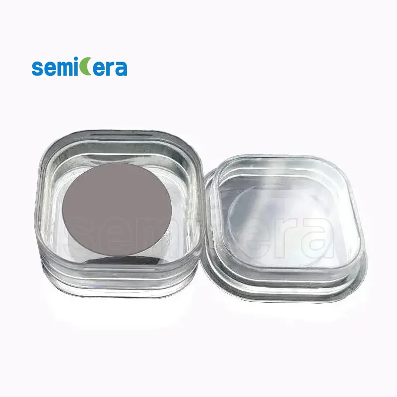
Seminer is proud to present the Substrat de galerie de nitrure d'aluminium de 30 mm, a top-tier material engineered to meet the stringent demands of modern electronic and optoelectronic applications. Aluminum Nitride (AlN) substrates are renowned for their outstanding thermal conductivity and electrical insulation properties, making them an ideal choice for high-performance devices.
Caractéristiques clés:
• Exceptional Thermal Conductivity: The Substrat de galerie de nitrure d'aluminium de 30 mm boasts a thermal conductivity of up to 170 W/mK, significantly higher than other substrate materials, ensuring efficient heat dissipation in high-power applications.
• High Electrical Insulation: With excellent electrical insulating properties, this substrate minimizes cross-talk and signal interference, making it ideal for RF and microwave applications.
• Résistance mécanique: The Substrat de galerie de nitrure d'aluminium de 30 mm offers superior mechanical strength and stability, ensuring durability and reliability even under rigorous operating conditions.
• Versatile Applications: This substrate is perfect for use in high-power LEDs, laser diodes, and RF components, providing a robust and reliable foundation for your most demanding projects.
• Precision Fabrication: Semicera ensures that each wafer substrate is fabricated with the highest precision, offering uniform thickness and surface quality to meet the exacting standards of advanced electronic devices.
Maximize the efficiency and reliability of your devices with Semicera’s Substrat de galerie de nitrure d'aluminium de 30 mm. Our substrates are designed to deliver superior performance, ensuring that your electronic and optoelectronic systems operate at their best. Trust Semicera for cutting-edge materials that lead the industry in quality and innovation.
|
Articles |
Production |
Recherche |
Factice |
|
Paramètres de cristal |
|||
|
Polytype |
4H |
||
|
Erreur d'orientation de la surface |
4±0.15° |
||
|
Paramètres électriques |
|||
|
Dopant |
azote de type N |
||
|
Résistivité |
0,015-0.025ohm · cm |
||
|
Paramètres mécaniques |
|||
|
Diamètre |
150,0 ± 0,2 mm |
||
|
Épaisseur |
350 ± 25 µm |
||
|
Orientation plate primaire |
[1-100]±5° |
||
|
Longueur plate primaire |
47,5 ± 1,5 mm |
||
|
Plat secondaire |
Aucun |
||
|
TTV |
≤5 µm |
≤10 µm |
≤15 µm |
|
LTV |
≤3 μm (5 mm * 5 mm) |
≤5 μm (5 mm * 5 mm) |
≤10 μm (5 mm * 5 mm) |
|
Arc |
-15 μm ~ 15μm |
-35 μm ~ 35 μm |
-45 μm ~ 45 μm |
|
Chaîne |
≤35 µm |
≤45 µm |
≤55 µm |
|
Rugosité avant (si-face) (AFM) |
Ra≤0,2 nm (5 μm * 5 μm) |
||
|
Structure |
|||
|
Densité de micro- |
<1 ea / cm2 |
<10 ea / cm2 |
<15 ea / cm2 |
|
Impuretés métalliques |
≤5E10atoms/cm2 |
N / A |
|
|
BPB |
≤1500 ea / cm2 |
≤3000 ea / cm2 |
N / A |
|
TSD |
≤500 ea / cm2 |
≤1000 ea / cm2 |
N / A |
|
Qualité avant |
|||
|
Devant |
Si |
||
|
Finition de surface |
CMP SI-FACE |
||
|
Particules |
≤60ea / plaquette (taille 0,3 μm) |
N / A |
|
|
Rayures |
≤5EA / MM. Longueur cumulative ≤ diamètre |
Longueur cumulatif ≤2 * diamètre |
N / A |
|
PELLE / PEPES ORANGE / TAPPES / COMMENTS / CRESCHES / CONTAMINATION |
Aucun |
N / A |
|
|
Coups de bord / retraits / fracture / plaques hexagonales |
Aucun |
||
|
Zones de polytype |
Aucun |
Zone cumulative≤20% |
Zone cumulative ≤ 30% |
|
Marquage laser avant |
Aucun |
||
|
Qualité du dos |
|||
|
Finition arrière |
CMP C-FACE |
||
|
Rayures |
≤5ea / mm, longueur cumulative≤2 * diamètre |
N / A |
|
|
Défauts arrière (puces de bord / retraits) |
Aucun |
||
|
Rugosité du dos |
Ra≤0,2 nm (5 μm * 5 μm) |
||
|
Marquage laser arrière |
1 mm (du bord supérieur) |
||
|
Bord |
|||
|
Bord |
Chanfreiner |
||
|
Conditionnement |
|||
|
Conditionnement |
Préparé en épi avec un emballage sous vide Emballage de cassette multi-wafer |
||
|
*Remarques: «NA» signifie qu'aucun élément de demande non mentionné ne peut se référer au semi-std. |
|||


