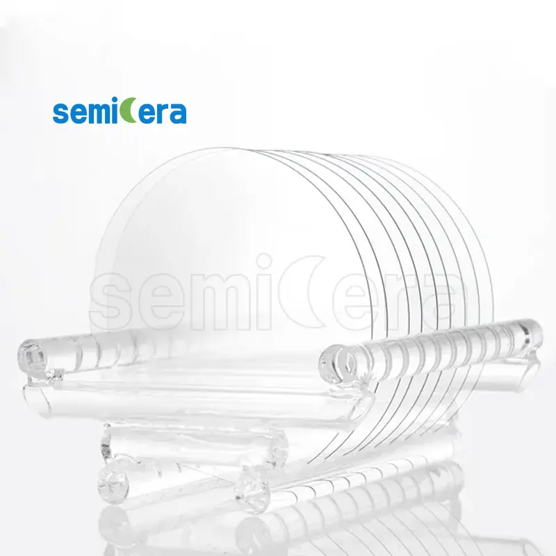
Semicera’s 4 Inch High Purity Semi-Insulating (HPSI) SiC Double-side Polished Wafer Substrates are crafted to meet the exacting demands of the semiconductor industry. These substrates are designed with exceptional flatness and purity, offering an optimal platform for cutting-edge electronic devices.
These HPSI SiC wafers are distinguished by their superior thermal conductivity and electrical insulation properties, making them an excellent choice for high-frequency and high-power applications. The double-side polishing process ensures minimal surface roughness, which is crucial for enhancing device performance and longevity.
The high purity of Semicera’s SiC wafers minimizes defects and impurities, leading to higher yield rates and device reliability. These substrates are suitable for a wide range of applications, including microwave devices, power electronics, and LED technologies, where precision and durability are essential.
With a focus on innovation and quality, Semicera utilizes advanced manufacturing techniques to produce wafers that meet the stringent requirements of modern electronics. The double-sided polishing not only improves the mechanical strength but also facilitates better integration with other semiconductor materials.
By choosing Semicera’s 4 Inch High Purity Semi-Insulating HPSI SiC Double-side Polished Wafer Substrates, manufacturers can leverage the benefits of enhanced thermal management and electrical insulation, paving the way for the development of more efficient and powerful electronic devices. Semicera continues to lead the industry with its commitment to quality and technological advancement.
|
Articles |
Production |
Recherche |
Factice |
|
Paramètres de cristal |
|||
|
Polytype |
4H |
||
|
Erreur d'orientation de la surface |
4±0.15° |
||
|
Paramètres électriques |
|||
|
Dopant |
azote de type N |
||
|
Résistivité |
0,015-0.025ohm · cm |
||
|
Paramètres mécaniques |
|||
|
Diamètre |
150,0 ± 0,2 mm |
||
|
Épaisseur |
350 ± 25 µm |
||
|
Orientation plate primaire |
[1-100]±5° |
||
|
Longueur plate primaire |
47,5 ± 1,5 mm |
||
|
Plat secondaire |
Aucun |
||
|
TTV |
≤5 µm |
≤10 µm |
≤15 µm |
|
LTV |
≤3 μm (5 mm * 5 mm) |
≤5 μm (5 mm * 5 mm) |
≤10 μm (5 mm * 5 mm) |
|
Arc |
-15 μm ~ 15μm |
-35 μm ~ 35 μm |
-45 μm ~ 45 μm |
|
Chaîne |
≤35 µm |
≤45 µm |
≤55 µm |
|
Rugosité avant (si-face) (AFM) |
Ra≤0,2 nm (5 μm * 5 μm) |
||
|
Structure |
|||
|
Densité de micro- |
<1 ea / cm2 |
<10 ea / cm2 |
<15 ea / cm2 |
|
Impuretés métalliques |
≤5E10atoms/cm2 |
N / A |
|
|
BPB |
≤1500 ea / cm2 |
≤3000 ea / cm2 |
N / A |
|
TSD |
≤500 ea / cm2 |
≤1000 ea / cm2 |
N / A |
|
Qualité avant |
|||
|
Devant |
Si |
||
|
Finition de surface |
CMP SI-FACE |
||
|
Particules |
≤60ea / plaquette (taille 0,3 μm) |
N / A |
|
|
Rayures |
≤5EA / MM. Longueur cumulative ≤ diamètre |
Longueur cumulatif ≤2 * diamètre |
N / A |
|
PELLE / PEPES ORANGE / TAPPES / COMMENTS / CRESCHES / CONTAMINATION |
Aucun |
N / A |
|
|
Coups de bord / retraits / fracture / plaques hexagonales |
Aucun |
||
|
Zones de polytype |
Aucun |
Zone cumulative≤20% |
Zone cumulative ≤ 30% |
|
Marquage laser avant |
Aucun |
||
|
Qualité du dos |
|||
|
Finition arrière |
CMP C-FACE |
||
|
Rayures |
≤5ea / mm, longueur cumulative≤2 * diamètre |
N / A |
|
|
Défauts arrière (puces de bord / retraits) |
Aucun |
||
|
Rugosité du dos |
Ra≤0,2 nm (5 μm * 5 μm) |
||
|
Marquage laser arrière |
1 mm (du bord supérieur) |
||
|
Bord |
|||
|
Bord |
Chanfreiner |
||
|
Conditionnement |
|||
|
Conditionnement |
Préparé en épi avec un emballage sous vide Emballage de cassette multi-wafer |
||
|
*Remarques: «NA» signifie qu'aucun élément de demande non mentionné ne peut se référer au semi-std. |
|||


