Silicon carbide (SiC) single crystal material has a large band gap width (~Si 3 times), high thermal conductivity (~Si 3.3 times or GaAs 10 times), high electron saturation migration rate (~Si 2.5 times), high breakdown electric field (~Si 10 times or GaAs 5 times) and other outstanding characteristics.
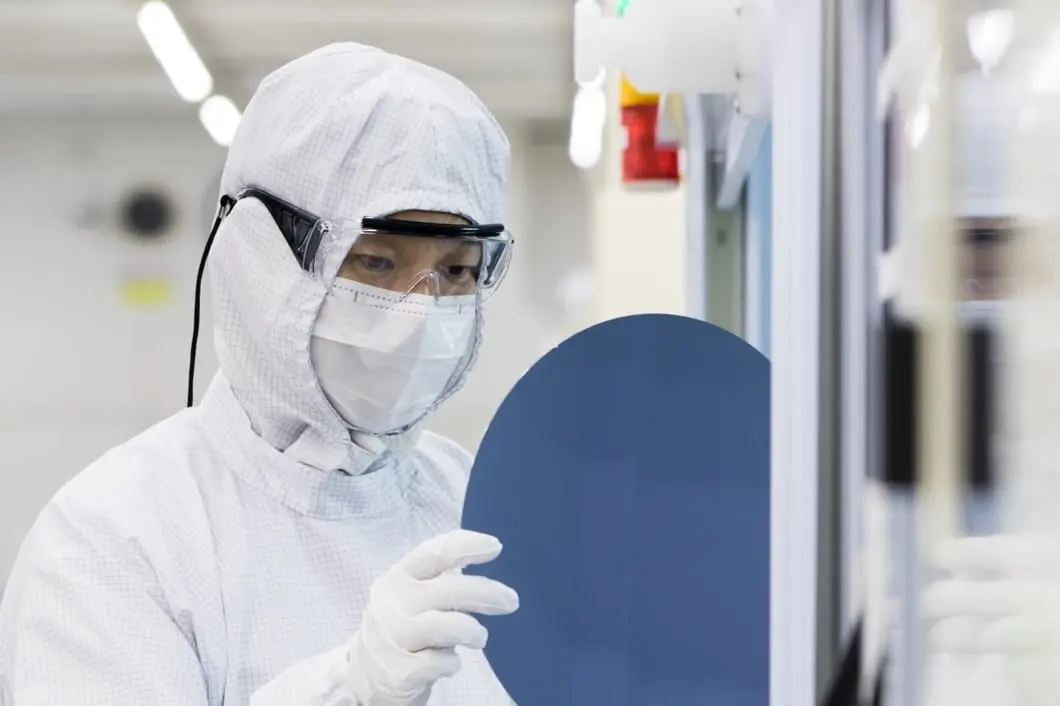
Semicera energy can provide customers with high-quality Conductive (Conductive), Semi-insulating (Semi-insulating), HPSI (High Purity semi-insulating) silicon carbide substrate; In addition, we can provide customers with homogeneous and heterogeneous silicon carbide epitaxial sheets; We can also customize the epitaxial sheet according to the specific needs of customers, and there is no minimum order quantity.
|
Articles |
Production |
Recherche |
Factice |
|
Paramètres de cristal |
|||
|
Polytype |
4H |
||
|
Erreur d'orientation de la surface |
<11-20 >4±0.15° |
||
|
Paramètres électriques |
|||
|
Dopant |
azote de type N |
||
|
Résistivité |
0.015-0.025ohm·cm |
||
|
Paramètres mécaniques |
|||
|
Diamètre |
99.5 – 100mm |
||
|
Épaisseur |
350±25 μm |
||
|
Orientation plate primaire |
[1-100]±5° |
||
|
Longueur plate primaire |
32.5±1.5mm |
||
|
Secondary flat position |
90° CW from primary flat ±5°. silicon face up |
||
|
Secondary flat length |
18±1.5mm |
||
|
TTV |
≤5 μm |
≤10 μm |
≤20 μm |
|
LTV |
≤2 μm(5mm*5mm) |
≤5 μm(5mm*5mm) |
N / A |
|
Arc |
-15μm ~ 15μm |
-35μm ~ 35μm |
-45μm ~ 45μm |
|
Chaîne |
≤20 μm |
≤45 μm |
≤50 μm |
|
Rugosité avant (si-face) (AFM) |
Ra≤0.2nm (5μm*5μm) |
||
|
Structure |
|||
|
Densité de micro- |
≤1 ea/cm2 |
≤5 ea/cm2 |
≤10 ea/cm2 |
|
Impuretés métalliques |
≤5E10atoms/cm2 |
N / A |
|
|
BPB |
≤1500 ea/cm2 |
≤3000 ea/cm2 |
N / A |
|
TSD |
≤500 ea/cm2 |
≤1000 ea/cm2 |
N / A |
|
Qualité avant |
|||
|
Devant |
Si |
||
|
Finition de surface |
CMP SI-FACE |
||
|
Particules |
≤60ea/wafer (size≥0.3μm) |
N / A |
|
|
Rayures |
≤2ea/mm. Cumulative length ≤Diameter |
Cumulative length≤2*Diameter |
N / A |
|
PELLE / PEPES ORANGE / TAPPES / COMMENTS / CRESCHES / CONTAMINATION |
Aucun |
N / A |
|
|
Coups de bord / retraits / fracture / plaques hexagonales |
Aucun |
N / A |
|
|
Zones de polytype |
Aucun |
Cumulative area≤20% |
Cumulative area≤30% |
|
Marquage laser avant |
Aucun |
||
|
Qualité du dos |
|||
|
Finition arrière |
CMP C-FACE |
||
|
Rayures |
≤5ea/mm,Cumulative length≤2*Diameter |
N / A |
|
|
Défauts arrière (puces de bord / retraits) |
Aucun |
||
|
Rugosité du dos |
Ra≤0.2nm (5μm*5μm) |
||
|
Marquage laser arrière |
1 mm (du bord supérieur) |
||
|
Bord |
|||
|
Bord |
Chanfreiner |
||
|
Conditionnement |
|||
|
Conditionnement |
The inner bag is filled with nitrogen and the outer bag is vacuumed. Multi-wafer cassette, epi-ready. |
||
|
*Remarques: «NA» signifie qu'aucun élément de demande non mentionné ne peut se référer au semi-std. |
|||