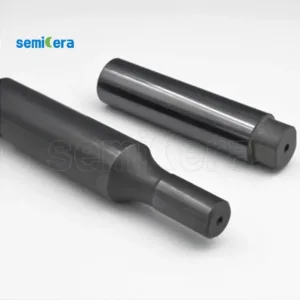
Seminer proudly presents its cutting-edge Gan Epitaxy services, designed to meet the ever-evolving needs of the semiconductor industry. Gallium nitride (GaN) is a material known for its exceptional properties, and our epitaxial growth processes ensure that these benefits are fully realized in your devices.
High-Performance GaN Layers Seminer specializes in the production of high-quality Gan Epitaxy layers, offering unparalleled material purity and structural integrity. These layers are critical for a variety of applications, from power electronics to optoelectronics, where superior performance and reliability are essential. Our precision growth techniques ensure that each GaN layer meets the exacting standards required for cutting-edge devices.
Optimized for Efficiency Le Gan Epitaxy provided by Semicera is specifically engineered to enhance the efficiency of your electronic components. By delivering low-defect, high-purity GaN layers, we enable devices to operate at higher frequencies and voltages, with reduced power loss. This optimization is key for applications such as high-electron-mobility transistors (HEMTs) and light-emitting diodes (LEDs), where efficiency is paramount.
Versatile Application Potential Seminer’s Gan Epitaxy is versatile, catering to a broad range of industries and applications. Whether you are developing power amplifiers, RF components, or laser diodes, our GaN epitaxial layers provide the foundation needed for high-performance, reliable devices. Our process can be tailored to meet specific requirements, ensuring that your products achieve optimal results.
Commitment to Quality Quality is the cornerstone of Seminer’s approach to Gan Epitaxy. We use advanced epitaxial growth technologies and rigorous quality control measures to produce GaN layers that exhibit excellent uniformity, low defect densities, and superior material properties. This commitment to quality ensures that your devices not only meet but exceed industry standards.
Innovative Growth Techniques Seminer is at the forefront of innovation in the field of Gan Epitaxy. Our team continuously explores new methods and technologies to improve the growth process, delivering GaN layers with enhanced electrical and thermal characteristics. These innovations translate into better-performing devices, capable of meeting the demands of next-generation applications.
Customized Solutions for Your Projects Recognizing that each project has unique requirements, Seminer offers customized Gan Epitaxy solutions. Whether you need specific doping profiles, layer thicknesses, or surface finishes, we work closely with you to develop a process that meets your exact needs. Our goal is to provide you with GaN layers that are precisely engineered to support your device’s performance and reliability.
|
Articles |
Production |
Recherche |
Factice |
|
Paramètres de cristal |
|||
|
Polytype |
4H |
||
|
Erreur d'orientation de la surface |
4±0.15° |
||
|
Paramètres électriques |
|||
|
Dopant |
azote de type N |
||
|
Résistivité |
0,015-0.025ohm · cm |
||
|
Paramètres mécaniques |
|||
|
Diamètre |
150,0 ± 0,2 mm |
||
|
Épaisseur |
350 ± 25 µm |
||
|
Orientation plate primaire |
[1-100]±5° |
||
|
Longueur plate primaire |
47,5 ± 1,5 mm |
||
|
Plat secondaire |
Aucun |
||
|
TTV |
≤5 µm |
≤10 µm |
≤15 µm |
|
LTV |
≤3 μm (5 mm * 5 mm) |
≤5 μm (5 mm * 5 mm) |
≤10 μm (5 mm * 5 mm) |
|
Arc |
-15 μm ~ 15μm |
-35 μm ~ 35 μm |
-45 μm ~ 45 μm |
|
Chaîne |
≤35 µm |
≤45 µm |
≤55 µm |
|
Rugosité avant (si-face) (AFM) |
Ra≤0,2 nm (5 μm * 5 μm) |
||
|
Structure |
|||
|
Densité de micro- |
<1 ea / cm2 |
<10 ea / cm2 |
<15 ea / cm2 |
|
Impuretés métalliques |
≤5E10atoms/cm2 |
N / A |
|
|
BPB |
≤1500 ea / cm2 |
≤3000 ea / cm2 |
N / A |
|
TSD |
≤500 ea / cm2 |
≤1000 ea / cm2 |
N / A |
|
Qualité avant |
|||
|
Devant |
Si |
||
|
Finition de surface |
CMP SI-FACE |
||
|
Particules |
≤60ea / plaquette (taille 0,3 μm) |
N / A |
|
|
Rayures |
≤5EA / MM. Longueur cumulative ≤ diamètre |
Longueur cumulatif ≤2 * diamètre |
N / A |
|
PELLE / PEPES ORANGE / TAPPES / COMMENTS / CRESCHES / CONTAMINATION |
Aucun |
N / A |
|
|
Coups de bord / retraits / fracture / plaques hexagonales |
Aucun |
||
|
Zones de polytype |
Aucun |
Zone cumulative≤20% |
Zone cumulative ≤ 30% |
|
Marquage laser avant |
Aucun |
||
|
Qualité du dos |
|||
|
Finition arrière |
CMP C-FACE |
||
|
Rayures |
≤5ea / mm, longueur cumulative≤2 * diamètre |
N / A |
|
|
Défauts arrière (puces de bord / retraits) |
Aucun |
||
|
Rugosité du dos |
Ra≤0,2 nm (5 μm * 5 μm) |
||
|
Marquage laser arrière |
1 mm (du bord supérieur) |
||
|
Bord |
|||
|
Bord |
Chanfreiner |
||
|
Conditionnement |
|||
|
Conditionnement |
Préparé en épi avec un emballage sous vide Emballage de cassette multi-wafer |
||
|
*Remarques: «NA» signifie qu'aucun élément de demande non mentionné ne peut se référer au semi-std. |
|||