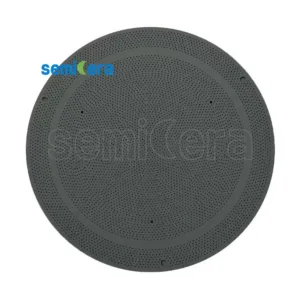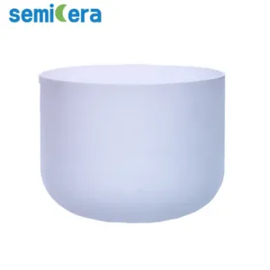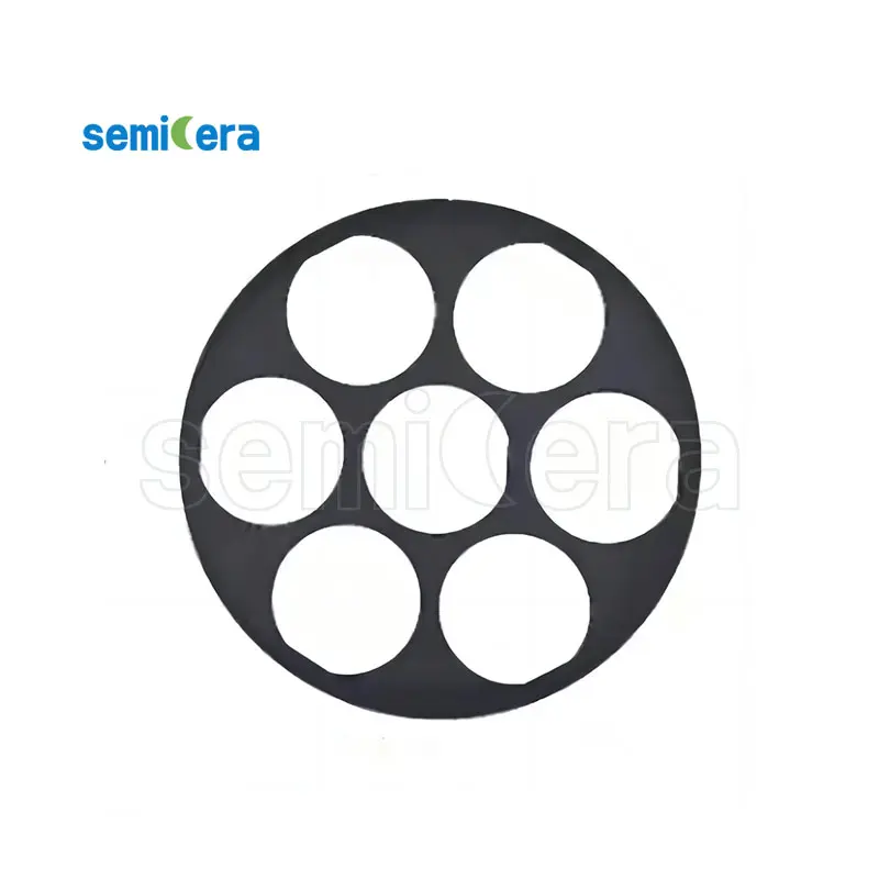
Product Description
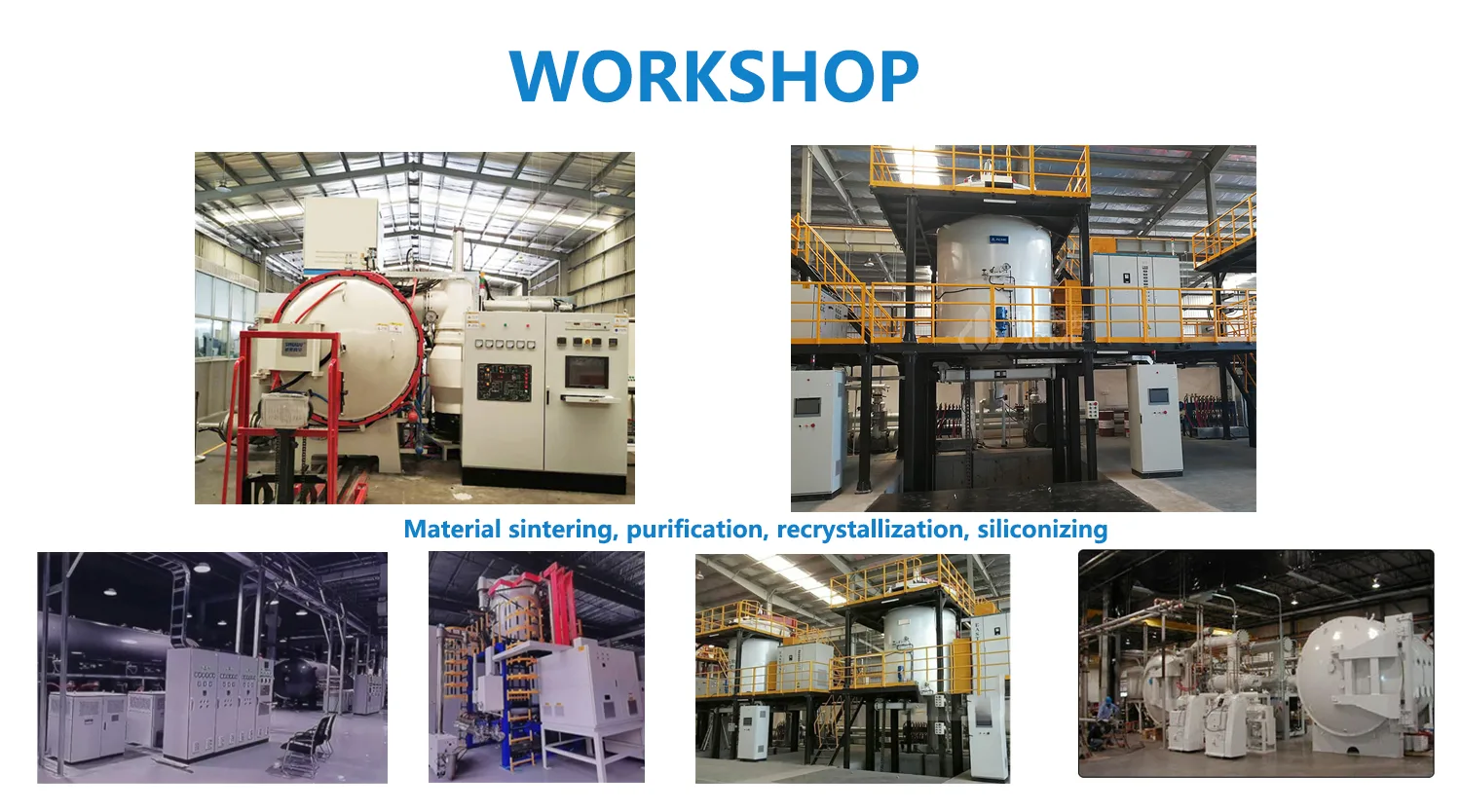
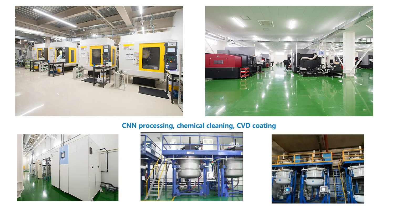
Our company provides SiC coating process services by CVD method on the surface of graphite, ceramics and other materials, so that special gases containing carbon and silicon react at high temperature to obtain high purity SiC molecules, molecules deposited on the surface of the coated materials, forming SIC protective layer.
Caractéristiques principales:
1. Résistance à l'oxydation à haute température:
La résistance à l'oxydation est encore très bonne lorsque la température est aussi élevée que 1600 C.
2. High purity : made by chemical vapor deposition under high temperature chlorination condition.
3. Résistance à l'érosion: dureté élevée, surface compacte, particules fines.
4. Résistance à la corrosion: réactifs acide, alcalin, sel et organique.


Spécifications principales du revêtement CVD-SIC
|
Propriétés SIC-CVD |
||
|
Structure cristalline |
Phase FCC β |
|
|
Densité |
g / cm ³ |
3.21 |
|
Dureté |
Vickers dureté |
2500 |
|
Taille des grains |
MM |
2~10 |
|
Pureté chimique |
% |
99.99995 |
|
Capacité thermique |
J · kg-1 · k-1 |
640 |
|
Température de sublimation |
℃ |
2700 |
|
Résistance aux félexes |
MPA (RT 4 points) |
415 |
|
Module de jeunes |
GPA (4pt Bend, 1300 ℃) |
430 |
|
Expansion thermique (CTE) |
10-6K-1 |
4.5 |
|
Conductivité thermique |
(W / mk) |
300 |