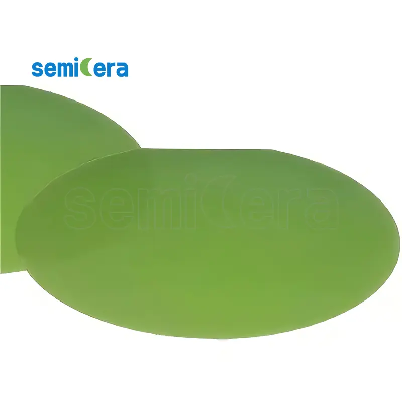
Semicera’s Silicon Carbide Epitaxy is engineered to meet the rigorous demands of modern semiconductor applications. By utilizing advanced epitaxial growth techniques, we ensure that each silicon carbide layer exhibits exceptional crystalline quality, uniformity, and minimal defect density. These characteristics are crucial for developing high-performance power electronics, where efficiency and thermal management are paramount.
Le Silicon Carbide Epitaxy process at Semicera is optimized to produce epitaxial layers with precise thickness and doping control, ensuring consistent performance across a range of devices. This level of precision is essential for applications in electric vehicles, renewable energy systems, and high-frequency communications, where reliability and efficiency are critical.
Moreover, Semicera’s Silicon Carbide Epitaxy offers enhanced thermal conductivity and higher breakdown voltage, making it the preferred choice for devices that operate under extreme conditions. These properties contribute to longer device lifetimes and improved overall system efficiency, particularly in high-power and high-temperature environments.
Semicera also provides customization options for Silicon Carbide Epitaxy, allowing for tailored solutions that meet specific device requirements. Whether for research or large-scale production, our epitaxial layers are designed to support the next generation of semiconductor innovations, enabling the development of more powerful, efficient, and reliable electronic devices.
By integrating cutting-edge technology and stringent quality control processes, Semicera ensures that our Silicon Carbide Epitaxy products not only meet but exceed industry standards. This commitment to excellence makes our epitaxial layers the ideal foundation for advanced semiconductor applications, paving the way for breakthroughs in power electronics and optoelectronics.
|
Articles |
Production |
Recherche |
Factice |
|
Paramètres de cristal |
|||
|
Polytype |
4H |
||
|
Erreur d'orientation de la surface |
4±0.15° |
||
|
Paramètres électriques |
|||
|
Dopant |
azote de type N |
||
|
Résistivité |
0,015-0.025ohm · cm |
||
|
Paramètres mécaniques |
|||
|
Diamètre |
150,0 ± 0,2 mm |
||
|
Épaisseur |
350 ± 25 µm |
||
|
Orientation plate primaire |
[1-100]±5° |
||
|
Longueur plate primaire |
47,5 ± 1,5 mm |
||
|
Plat secondaire |
Aucun |
||
|
TTV |
≤5 µm |
≤10 µm |
≤15 µm |
|
LTV |
≤3 μm (5 mm * 5 mm) |
≤5 μm (5 mm * 5 mm) |
≤10 μm (5 mm * 5 mm) |
|
Arc |
-15 μm ~ 15μm |
-35 μm ~ 35 μm |
-45 μm ~ 45 μm |
|
Chaîne |
≤35 µm |
≤45 µm |
≤55 µm |
|
Rugosité avant (si-face) (AFM) |
Ra≤0,2 nm (5 μm * 5 μm) |
||
|
Structure |
|||
|
Densité de micro- |
<1 ea / cm2 |
<10 ea / cm2 |
<15 ea / cm2 |
|
Impuretés métalliques |
≤5E10atoms/cm2 |
N / A |
|
|
BPB |
≤1500 ea / cm2 |
≤3000 ea / cm2 |
N / A |
|
TSD |
≤500 ea / cm2 |
≤1000 ea / cm2 |
N / A |
|
Qualité avant |
|||
|
Devant |
Si |
||
|
Finition de surface |
CMP SI-FACE |
||
|
Particules |
≤60ea / plaquette (taille 0,3 μm) |
N / A |
|
|
Rayures |
≤5EA / MM. Longueur cumulative ≤ diamètre |
Longueur cumulatif ≤2 * diamètre |
N / A |
|
PELLE / PEPES ORANGE / TAPPES / COMMENTS / CRESCHES / CONTAMINATION |
Aucun |
N / A |
|
|
Coups de bord / retraits / fracture / plaques hexagonales |
Aucun |
||
|
Zones de polytype |
Aucun |
Zone cumulative≤20% |
Zone cumulative ≤ 30% |
|
Marquage laser avant |
Aucun |
||
|
Qualité du dos |
|||
|
Finition arrière |
CMP C-FACE |
||
|
Rayures |
≤5ea / mm, longueur cumulative≤2 * diamètre |
N / A |
|
|
Défauts arrière (puces de bord / retraits) |
Aucun |
||
|
Rugosité du dos |
Ra≤0,2 nm (5 μm * 5 μm) |
||
|
Marquage laser arrière |
1 mm (du bord supérieur) |
||
|
Bord |
|||
|
Bord |
Chanfreiner |
||
|
Conditionnement |
|||
|
Conditionnement |
Préparé en épi avec un emballage sous vide Emballage de cassette multi-wafer |
||
|
*Remarques: «NA» signifie qu'aucun élément de demande non mentionné ne peut se référer au semi-std. |
|||