Semicera Silicon Substrates are crafted to meet the rigorous demands of the semiconductor industry, offering unparalleled quality and precision. These substrates provide a reliable foundation for various applications, from integrated circuits to photovoltaic cells, ensuring optimal performance and longevity.
The high purity of Semicera Silicon Substrates ensures minimal defects and superior electrical characteristics, which are critical for the production of high-efficiency electronic components. This level of purity helps in reducing energy loss and improving the overall efficiency of semiconductor devices.
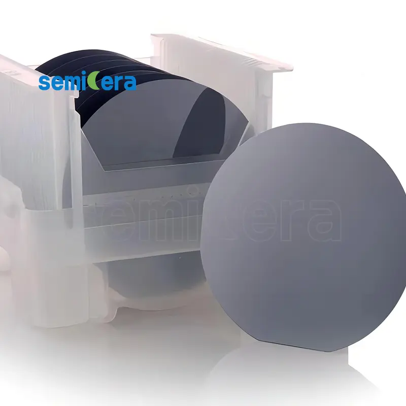
Semicera employs state-of-the-art manufacturing techniques to produce silicon substrates with exceptional uniformity and flatness. This precision is essential for achieving consistent results in semiconductor fabrication, where even the slightest variation can impact device performance and yield.
Available in a variety of sizes and specifications, Semicera Silicon Substrates cater to a wide range of industrial needs. Whether you are developing cutting-edge microprocessors or solar panels, these substrates provide the flexibility and reliability required for your specific application.
Semicera is dedicated to supporting innovation and efficiency in the semiconductor industry. By providing high-quality silicon substrates, we enable manufacturers to push the boundaries of technology, delivering products that meet the evolving demands of the market. Trust Semicera for your next-generation electronic and photovoltaic solutions.
|
Articles |
Production |
Recherche |
Factice |
|
Paramètres de cristal |
|||
|
Polytype |
4H |
||
|
Erreur d'orientation de la surface |
4±0.15° |
||
|
Paramètres électriques |
|||
|
Dopant |
azote de type N |
||
|
Résistivité |
0,015-0.025ohm · cm |
||
|
Paramètres mécaniques |
|||
|
Diamètre |
150,0 ± 0,2 mm |
||
|
Épaisseur |
350 ± 25 µm |
||
|
Orientation plate primaire |
[1-100]±5° |
||
|
Longueur plate primaire |
47,5 ± 1,5 mm |
||
|
Plat secondaire |
Aucun |
||
|
TTV |
≤5 µm |
≤10 µm |
≤15 µm |
|
LTV |
≤3 μm (5 mm * 5 mm) |
≤5 μm (5 mm * 5 mm) |
≤10 μm (5 mm * 5 mm) |
|
Arc |
-15 μm ~ 15μm |
-35 μm ~ 35 μm |
-45 μm ~ 45 μm |
|
Chaîne |
≤35 µm |
≤45 µm |
≤55 µm |
|
Rugosité avant (si-face) (AFM) |
Ra≤0,2 nm (5 μm * 5 μm) |
||
|
Structure |
|||
|
Densité de micro- |
<1 ea / cm2 |
<10 ea / cm2 |
<15 ea / cm2 |
|
Impuretés métalliques |
≤5E10atoms/cm2 |
N / A |
|
|
BPB |
≤1500 ea / cm2 |
≤3000 ea / cm2 |
N / A |
|
TSD |
≤500 ea / cm2 |
≤1000 ea / cm2 |
N / A |
|
Qualité avant |
|||
|
Devant |
Si |
||
|
Finition de surface |
CMP SI-FACE |
||
|
Particules |
≤60ea / plaquette (taille 0,3 μm) |
N / A |
|
|
Rayures |
≤5EA / MM. Longueur cumulative ≤ diamètre |
Longueur cumulatif ≤2 * diamètre |
N / A |
|
PELLE / PEPES ORANGE / TAPPES / COMMENTS / CRESCHES / CONTAMINATION |
Aucun |
N / A |
|
|
Coups de bord / retraits / fracture / plaques hexagonales |
Aucun |
||
|
Zones de polytype |
Aucun |
Zone cumulative≤20% |
Zone cumulative ≤ 30% |
|
Marquage laser avant |
Aucun |
||
|
Qualité du dos |
|||
|
Finition arrière |
CMP C-FACE |
||
|
Rayures |
≤5ea / mm, longueur cumulative≤2 * diamètre |
N / A |
|
|
Défauts arrière (puces de bord / retraits) |
Aucun |
||
|
Rugosité du dos |
Ra≤0,2 nm (5 μm * 5 μm) |
||
|
Marquage laser arrière |
1 mm (du bord supérieur) |
||
|
Bord |
|||
|
Bord |
Chanfreiner |
||
|
Conditionnement |
|||
|
Conditionnement |
Préparé en épi avec un emballage sous vide Emballage de cassette multi-wafer |
||
|
*Remarques: «NA» signifie qu'aucun élément de demande non mentionné ne peut se référer au semi-std. |
|||


