Semicera is proud to present the Ga2O3 Substrate, a cutting-edge material poised to revolutionize power electronics and optoelectronics. Gallium Oxide (Ga2O3) substrates are known for their ultra-wide bandgap, making them ideal for high-power and high-frequency devices.
Caratteristiche chiave:
• Ultra-Wide Bandgap: Ga2O3 offers a bandgap of approximately 4.8 eV, significantly enhancing its ability to handle high voltages and temperatures compared to traditional materials like Silicon and GaN.
• High Breakdown Voltage: With an exceptional breakdown field, the Ga2O3 Substrate is perfect for devices requiring high-voltage operation, ensuring greater efficiency and reliability.
• Thermal Stability: The material’s superior thermal stability makes it suitable for applications in extreme environments, maintaining performance even under harsh conditions.
• Versatile Applications: Ideal for use in high-efficiency power transistors, UV optoelectronic devices, and more, providing a robust foundation for advanced electronic systems.
Experience the future of semiconductor technology with Semicera’s Ga2O3 Substrate. Designed to meet the growing demands of high-power and high-frequency electronics, this substrate sets a new standard for performance and durability. Trust Semicera to deliver innovative solutions for your most challenging applications.
|
Elementi |
Produzione |
Ricerca |
Manichino |
|
Parametri cristallini |
|||
|
Politipo |
4H |
||
|
Errore di orientamento della superficie |
4±0.15° |
||
|
Parametri elettrici |
|||
|
Drogante |
azoto di tipo n |
||
|
Resistività |
0,015-0,025ohm · cm |
||
|
Parametri meccanici |
|||
|
Diametro |
150,0 ± 0,2 mm |
||
|
Spessore |
350 ± 25 µm |
||
|
Orientamento piatto primario |
[1-100]±5° |
||
|
Lunghezza piatta primaria |
47,5 ± 1,5 mm |
||
|
Piatto secondario |
Nessuno |
||
|
TTV |
≤5 µm |
≤10 µm |
≤15 µm |
|
LTV |
≤3 μm (5mm*5mm) |
≤5 μm (5 mm*5 mm) |
≤10 μm (5 mm*5 mm) |
|
Arco |
-15μm ~ 15μm |
-35μm ~ 35 μm |
-45μm ~ 45μm |
|
Ordito |
≤35 µm |
≤45 µm |
≤55 µm |
|
Front (Si-Face) Rughess (AFM) |
RA≤0,2 nm (5μm*5μm) |
||
|
Struttura |
|||
|
Densità di micrivipe |
<1 ea/cm2 |
<10 ea/cm2 |
<15 ea/cm2 |
|
Impurità dei metalli |
≤5E10atoms/cm2 |
N / A |
|
|
BPD |
≤1500 ea/cm2 |
≤3000 ea/cm2 |
N / A |
|
TSD |
≤500 ea/cm2 |
≤1000 ea/cm2 |
N / A |
|
Qualità anteriore |
|||
|
Davanti |
Si |
||
|
Finitura superficiale |
Si-Face CMP |
||
|
Particelle |
≤60ea/wafer (dimensione≥0,3μm) |
N / A |
|
|
Graffi |
≤5ea/mm. Lunghezza cumulativa ≤Diameter |
Diametro cumulativo della lunghezza ≤2* |
N / A |
|
Buccia/pozzi/macchie/striature/crepe/contaminazione |
Nessuno |
N / A |
|
|
Bordo chips/riendi/frattura/piastre esadecimale |
Nessuno |
||
|
Aree politepi |
Nessuno |
Area cumulativa≤20% |
Area cumulativa≤30% |
|
Marcatura laser anteriore |
Nessuno |
||
|
Qualità alla schiena |
|||
|
Finitura posteriore |
C-FACE CMP |
||
|
Graffi |
≤5ea/mm, lunghezza cumulativa≤2*diametro |
N / A |
|
|
Difetti posteriori (bordo chip/rientri) |
Nessuno |
||
|
Rugosità posteriore |
RA≤0,2 nm (5μm*5μm) |
||
|
Marcatura laser sul retro |
1 mm (dal bordo superiore) |
||
|
Bordo |
|||
|
Bordo |
Smussare |
||
|
Confezione |
|||
|
Confezione |
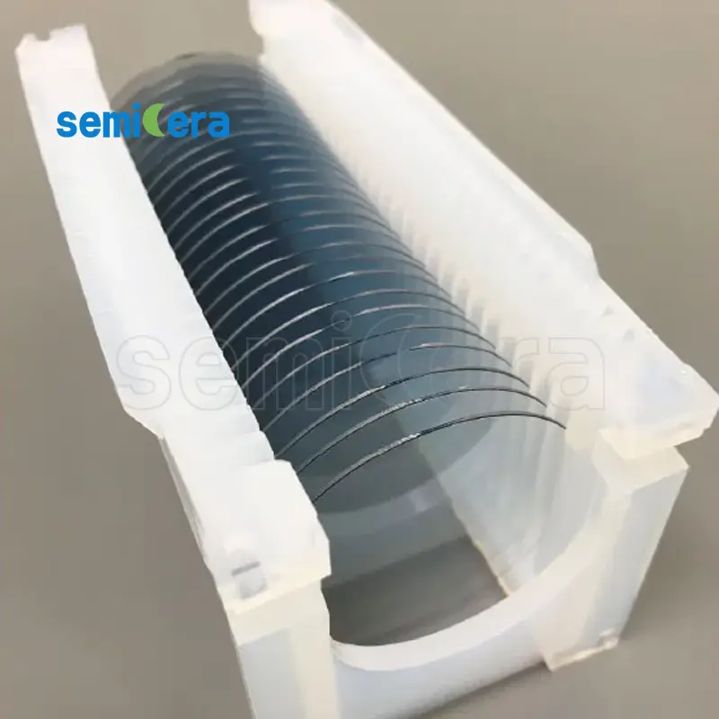
Prepasto EPI con imballaggio a vuoto Packaging a cassette multi-wafer |
||
|
*Note : “NA” significa che nessuna richiesta di richiesta non menzionata può fare riferimento a semi-std. |
|||


