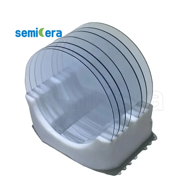
Semicera proudly introduces its 4″ Gallium Oxide Substrates, a groundbreaking material engineered to meet the growing demands of high-performance semiconductor devices. Gallium Oxide (Ga2O3) substrates offer an ultra-wide bandgap, making them ideal for next-generation power electronics, UV optoelectronics, and high-frequency devices.
Caratteristiche chiave:
• Ultra-Wide Bandgap: IL 4″ Gallium Oxide Substrates boast a bandgap of approximately 4.8 eV, allowing for exceptional voltage and temperature tolerance, significantly outperforming traditional semiconductor materials like silicon.
• High Breakdown Voltage: These substrates enable devices to operate at higher voltages and powers, making them perfect for high-voltage applications in power electronics.
• Superior Thermal Stability: Gallium Oxide substrates offer excellent thermal conductivity, ensuring stable performance under extreme conditions, ideal for use in demanding environments.
• High Material Quality: With low defect densities and high crystal quality, these substrates ensure reliable and consistent performance, enhancing the efficiency and durability of your devices.
• Versatile Application: Suitable for a wide range of applications, including power transistors, Schottky diodes, and UV-C LED devices, enabling innovations in both power and optoelectronic fields.
Explore the future of semiconductor technology with Semicera’s 4″ Gallium Oxide Substrates. Our substrates are designed to support the most advanced applications, providing the reliability and efficiency required for today’s cutting-edge devices. Trust Semicera for quality and innovation in your semiconductor materials.
|
Elementi |
Produzione |
Ricerca |
Manichino |
|
Parametri cristallini |
|||
|
Politipo |
4H |
||
|
Errore di orientamento della superficie |
4±0.15° |
||
|
Parametri elettrici |
|||
|
Drogante |
azoto di tipo n |
||
|
Resistività |
0,015-0,025ohm · cm |
||
|
Parametri meccanici |
|||
|
Diametro |
150,0 ± 0,2 mm |
||
|
Spessore |
350 ± 25 µm |
||
|
Orientamento piatto primario |
[1-100]±5° |
||
|
Lunghezza piatta primaria |
47,5 ± 1,5 mm |
||
|
Piatto secondario |
Nessuno |
||
|
TTV |
≤5 µm |
≤10 µm |
≤15 µm |
|
LTV |
≤3 μm (5mm*5mm) |
≤5 μm (5 mm*5 mm) |
≤10 μm (5 mm*5 mm) |
|
Arco |
-15μm ~ 15μm |
-35μm ~ 35 μm |
-45μm ~ 45μm |
|
Ordito |
≤35 µm |
≤45 µm |
≤55 µm |
|
Front (Si-Face) Rughess (AFM) |
RA≤0,2 nm (5μm*5μm) |
||
|
Struttura |
|||
|
Densità di micrivipe |
<1 ea/cm2 |
<10 ea/cm2 |
<15 ea/cm2 |
|
Impurità dei metalli |
≤5E10atoms/cm2 |
N / A |
|
|
BPD |
≤1500 ea/cm2 |
≤3000 ea/cm2 |
N / A |
|
TSD |
≤500 ea/cm2 |
≤1000 ea/cm2 |
N / A |
|
Qualità anteriore |
|||
|
Davanti |
Si |
||
|
Finitura superficiale |
Si-Face CMP |
||
|
Particelle |
≤60ea/wafer (dimensione≥0,3μm) |
N / A |
|
|
Graffi |
≤5ea/mm. Lunghezza cumulativa ≤Diameter |
Diametro cumulativo della lunghezza ≤2* |
N / A |
|
Buccia/pozzi/macchie/striature/crepe/contaminazione |
Nessuno |
N / A |
|
|
Bordo chips/riendi/frattura/piastre esadecimale |
Nessuno |
||
|
Aree politepi |
Nessuno |
Area cumulativa≤20% |
Area cumulativa≤30% |
|
Marcatura laser anteriore |
Nessuno |
||
|
Qualità alla schiena |
|||
|
Finitura posteriore |
C-FACE CMP |
||
|
Graffi |
≤5ea/mm, lunghezza cumulativa≤2*diametro |
N / A |
|
|
Difetti posteriori (bordo chip/rientri) |
Nessuno |
||
|
Rugosità posteriore |
RA≤0,2 nm (5μm*5μm) |
||
|
Marcatura laser sul retro |
1 mm (dal bordo superiore) |
||
|
Bordo |
|||
|
Bordo |
Smussare |
||
|
Confezione |
|||
|
Confezione |
Prepasto EPI con imballaggio a vuoto Packaging a cassette multi-wafer |
||
|
*Note : “NA” significa che nessuna richiesta di richiesta non menzionata può fare riferimento a semi-std. |
|||


