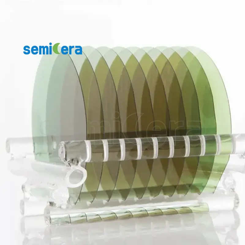
Semicera’s 6 Inch N-type SiC Wafer stands at the forefront of semiconductor technology. Crafted for optimal performance, this wafer excels in high-power, high-frequency, and high-temperature applications, essential for advanced electronic devices.
Our 6 Inch N-type SiC wafer features high electron mobility and low on-resistance, which are critical parameters for power devices such as MOSFETs, diodes, and other components. These properties ensure efficient energy conversion and reduced heat generation, enhancing the performance and lifespan of electronic systems.
Semicera’s rigorous quality control processes ensure that each SiC wafer maintains excellent surface flatness and minimal defects. This meticulous attention to detail ensures that our wafers meet the stringent requirements of industries such as automotive, aerospace, and telecommunications.
In addition to its superior electrical properties, the N-type SiC wafer offers robust thermal stability and resistance to high temperatures, making it ideal for environments where conventional materials might fail. This capability is particularly valuable in applications involving high-frequency and high-power operations.
By choosing Semicera’s 6 Inch N-type SiC Wafer, you are investing in a product that represents the pinnacle of semiconductor innovation. We are committed to providing the building blocks for cutting-edge devices, ensuring that our partners in various industries have access to the best materials for their technological advancements.
|
Elementi |
Produzione |
Ricerca |
Manichino |
|
Parametri cristallini |
|||
|
Politipo |
4H |
||
|
Errore di orientamento della superficie |
4±0.15° |
||
|
Parametri elettrici |
|||
|
Drogante |
azoto di tipo n |
||
|
Resistività |
0,015-0,025ohm · cm |
||
|
Parametri meccanici |
|||
|
Diametro |
150,0 ± 0,2 mm |
||
|
Spessore |
350 ± 25 µm |
||
|
Orientamento piatto primario |
[1-100]±5° |
||
|
Lunghezza piatta primaria |
47,5 ± 1,5 mm |
||
|
Piatto secondario |
Nessuno |
||
|
TTV |
≤5 µm |
≤10 µm |
≤15 µm |
|
LTV |
≤3 μm (5mm*5mm) |
≤5 μm (5 mm*5 mm) |
≤10 μm (5 mm*5 mm) |
|
Arco |
-15μm ~ 15μm |
-35μm ~ 35 μm |
-45μm ~ 45μm |
|
Ordito |
≤35 µm |
≤45 µm |
≤55 µm |
|
Front (Si-Face) Rughess (AFM) |
RA≤0,2 nm (5μm*5μm) |
||
|
Struttura |
|||
|
Densità di micrivipe |
<1 ea/cm2 |
<10 ea/cm2 |
<15 ea/cm2 |
|
Impurità dei metalli |
≤5E10atoms/cm2 |
N / A |
|
|
BPD |
≤1500 ea/cm2 |
≤3000 ea/cm2 |
N / A |
|
TSD |
≤500 ea/cm2 |
≤1000 ea/cm2 |
N / A |
|
Qualità anteriore |
|||
|
Davanti |
Si |
||
|
Finitura superficiale |
Si-Face CMP |
||
|
Particelle |
≤60ea/wafer (dimensione≥0,3μm) |
N / A |
|
|
Graffi |
≤5ea/mm. Lunghezza cumulativa ≤Diameter |
Diametro cumulativo della lunghezza ≤2* |
N / A |
|
Buccia/pozzi/macchie/striature/crepe/contaminazione |
Nessuno |
N / A |
|
|
Bordo chips/riendi/frattura/piastre esadecimale |
Nessuno |
||
|
Aree politepi |
Nessuno |
Area cumulativa≤20% |
Area cumulativa≤30% |
|
Marcatura laser anteriore |
Nessuno |
||
|
Qualità alla schiena |
|||
|
Finitura posteriore |
C-FACE CMP |
||
|
Graffi |
≤5ea/mm, lunghezza cumulativa≤2*diametro |
N / A |
|
|
Difetti posteriori (bordo chip/rientri) |
Nessuno |
||
|
Rugosità posteriore |
RA≤0,2 nm (5μm*5μm) |
||
|
Marcatura laser sul retro |
1 mm (dal bordo superiore) |
||
|
Bordo |
|||
|
Bordo |
Smussare |
||
|
Confezione |
|||
|
Confezione |
Prepasto EPI con imballaggio a vuoto Packaging a cassette multi-wafer |
||
|
*Note : “NA” significa che nessuna richiesta di richiesta non menzionata può fare riferimento a semi-std. |
|||


