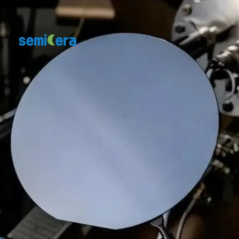
Semicera proudly offers Ga2O3 Epitaxy, a state-of-the-art solution designed to push the boundaries of power electronics and optoelectronics. This advanced epitaxial technology leverages the unique properties of Gallium Oxide (Ga2O3) to deliver superior performance in demanding applications.
Caratteristiche chiave:
• Exceptional Wide Bandgap: Ga2O3 Epitaxy features an ultra-wide bandgap, allowing for higher breakdown voltages and efficient operation in high-power environments.
• Alta conduttività termica: The epitaxial layer provides excellent thermal conductivity, ensuring stable operation even under high-temperature conditions, making it ideal for high-frequency devices.
• Superior Material Quality: Achieve high crystal quality with minimal defects, ensuring optimal device performance and longevity, especially in critical applications such as power transistors and UV detectors.
• Versatility in Applications: Perfectly suited for power electronics, RF applications, and optoelectronics, providing a reliable foundation for next-generation semiconductor devices.
Discover the potential of Ga2O3 Epitaxy with Semicera’s innovative solutions. Our epitaxial products are designed to meet the highest standards of quality and performance, enabling your devices to operate with maximum efficiency and reliability. Choose Semicera for cutting-edge semiconductor technology.
|
Elementi |
Produzione |
Ricerca |
Manichino |
|
Parametri cristallini |
|||
|
Politipo |
4H |
||
|
Errore di orientamento della superficie |
4±0.15° |
||
|
Parametri elettrici |
|||
|
Drogante |
azoto di tipo n |
||
|
Resistività |
0,015-0,025ohm · cm |
||
|
Parametri meccanici |
|||
|
Diametro |
150,0 ± 0,2 mm |
||
|
Spessore |
350 ± 25 µm |
||
|
Orientamento piatto primario |
[1-100]±5° |
||
|
Lunghezza piatta primaria |
47,5 ± 1,5 mm |
||
|
Piatto secondario |
Nessuno |
||
|
TTV |
≤5 µm |
≤10 µm |
≤15 µm |
|
LTV |
≤3 μm (5mm*5mm) |
≤5 μm (5 mm*5 mm) |
≤10 μm (5 mm*5 mm) |
|
Arco |
-15μm ~ 15μm |
-35μm ~ 35 μm |
-45μm ~ 45μm |
|
Ordito |
≤35 µm |
≤45 µm |
≤55 µm |
|
Front (Si-Face) Rughess (AFM) |
RA≤0,2 nm (5μm*5μm) |
||
|
Struttura |
|||
|
Densità di micrivipe |
<1 ea/cm2 |
<10 ea/cm2 |
<15 ea/cm2 |
|
Impurità dei metalli |
≤5E10atoms/cm2 |
N / A |
|
|
BPD |
≤1500 ea/cm2 |
≤3000 ea/cm2 |
N / A |
|
TSD |
≤500 ea/cm2 |
≤1000 ea/cm2 |
N / A |
|
Qualità anteriore |
|||
|
Davanti |
Si |
||
|
Finitura superficiale |
Si-Face CMP |
||
|
Particelle |
≤60ea/wafer (dimensione≥0,3μm) |
N / A |
|
|
Graffi |
≤5ea/mm. Lunghezza cumulativa ≤Diameter |
Diametro cumulativo della lunghezza ≤2* |
N / A |
|
Buccia/pozzi/macchie/striature/crepe/contaminazione |
Nessuno |
N / A |
|
|
Bordo chips/riendi/frattura/piastre esadecimale |
Nessuno |
||
|
Aree politepi |
Nessuno |
Area cumulativa≤20% |
Area cumulativa≤30% |
|
Marcatura laser anteriore |
Nessuno |
||
|
Qualità alla schiena |
|||
|
Finitura posteriore |
C-FACE CMP |
||
|
Graffi |
≤5ea/mm, lunghezza cumulativa≤2*diametro |
N / A |
|
|
Difetti posteriori (bordo chip/rientri) |
Nessuno |
||
|
Rugosità posteriore |
RA≤0,2 nm (5μm*5μm) |
||
|
Marcatura laser sul retro |
1 mm (dal bordo superiore) |
||
|
Bordo |
|||
|
Bordo |
Smussare |
||
|
Confezione |
|||
|
Confezione |
Prepasto EPI con imballaggio a vuoto Packaging a cassette multi-wafer |
||
|
*Note : “NA” significa che nessuna richiesta di richiesta non menzionata può fare riferimento a semi-std. |
|||