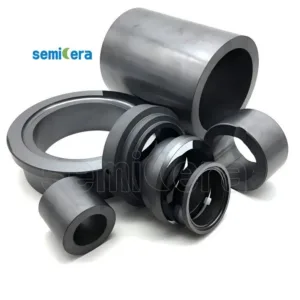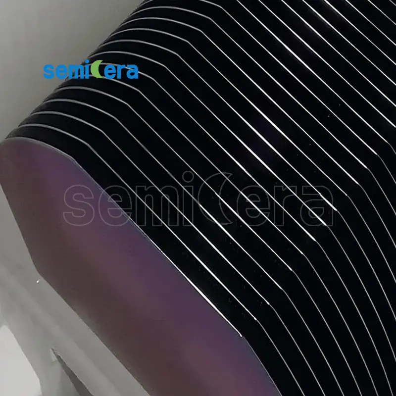
Silicon on Insulator Wafers from Semicera are designed to meet the growing demand for high-performance semiconductor solutions. Our SOI wafers offer superior electrical performance and reduced parasitic device capacitance, making them ideal for advanced applications such as MEMS devices, sensors, and integrated circuits. Semicera’s expertise in wafer production ensures that each SOI wafer provides reliable, high-quality results for your next-generation technology needs.
Our Silicon on Insulator Wafers offer an optimal balance between cost-effectiveness and performance. With soi wafer cost becoming increasingly competitive, these wafers are widely used in a range of industries, including microelectronics and optoelectronics. Semicera’s high-precision production process guarantees superior wafer bonding and uniformity, making them suitable for a variety of applications, from cavity SOI wafers to standard silicon wafers.
Caratteristiche chiave:
• Wafer SOI di alta qualità ottimizzati per le prestazioni in MEMS e altre applicazioni.
• Costo competitivo del wafer SOI per le aziende in cerca di soluzioni avanzate senza compromettere la qualità.
• Ideale per le tecnologie all'avanguardia, offrendo un migliore isolamento elettrico ed efficienza nel silicio sui sistemi di isolanti.
Our Silicon on Insulator Wafers are engineered to provide high-performance solutions, supporting the next wave of innovation in semiconductor technology. Whether you’re working on cavity SOI wafers, MEMS devices, or silicon on insulator components, Semicera delivers wafers that meet the highest standards in the industry.
|
Elementi |
Produzione |
Ricerca |
Manichino |
|
Parametri cristallini |
|||
|
Politipo |
4H |
||
|
Errore di orientamento della superficie |
<11-20 >4±0.15° |
||
|
Parametri elettrici |
|||
|
Drogante |
azoto di tipo n |
||
|
Resistività |
0.015-0.025ohm·cm |
||
|
Parametri meccanici |
|||
|
Diametro |
150.0±0.2mm |
||
|
Spessore |
350±25 μm |
||
|
Orientamento piatto primario |
[1-100]±5° |
||
|
Lunghezza piatta primaria |
47.5±1.5mm |
||
|
Piatto secondario |
Nessuno |
||
|
TTV |
≤5 μm |
≤10 μm |
≤15 μm |
|
LTV |
≤3 μm(5mm*5mm) |
≤5 μm(5mm*5mm) |
≤10 μm(5mm*5mm) |
|
Arco |
-15μm ~ 15μm |
-35μm ~ 35μm |
-45μm ~ 45μm |
|
Ordito |
≤35 μm |
≤45 μm |
≤55 μm |
|
Front (Si-Face) Rughess (AFM) |
Ra≤0.2nm (5μm*5μm) |
||
|
Struttura |
|||
|
Densità di micrivipe |
<1 ea/cm2 |
<10 ea/cm2 |
<15 ea/cm2 |
|
Impurità dei metalli |
≤5E10atoms/cm2 |
N / A |
|
|
BPD |
≤1500 ea/cm2 |
≤3000 ea/cm2 |
N / A |
|
TSD |
≤500 ea/cm2 |
≤1000 ea/cm2 |
N / A |
|
Qualità anteriore |
|||
|
Davanti |
Si |
||
|
Finitura superficiale |
Si-Face CMP |
||
|
Particelle |
≤60ea/wafer (size≥0.3μm) |
N / A |
|
|
Graffi |
≤5ea/mm. Cumulative length ≤Diameter |
Cumulative length≤2*Diameter |
N / A |
|
Buccia/pozzi/macchie/striature/crepe/contaminazione |
Nessuno |
N / A |
|
|
Bordo chips/riendi/frattura/piastre esadecimale |
Nessuno |
||
|
Aree politepi |
Nessuno |
Cumulative area≤20% |
Cumulative area≤30% |
|
Marcatura laser anteriore |
Nessuno |
||
|
Qualità alla schiena |
|||
|
Finitura posteriore |
C-FACE CMP |
||
|
Graffi |
≤5ea/mm,Cumulative length≤2*Diameter |
N / A |
|
|
Difetti posteriori (bordo chip/rientri) |
Nessuno |
||
|
Rugosità posteriore |
Ra≤0.2nm (5μm*5μm) |
||
|
Marcatura laser sul retro |
1 mm (dal bordo superiore) |
||
|
Bordo |
|||
|
Bordo |
Smussare |
||
|
Confezione |
|||
|
Confezione |
Prepasto EPI con imballaggio a vuoto Packaging a cassette multi-wafer |
||
|
*Notes: “NA” means no request Items not mentioned may refer to SEMI-STD. |
|||