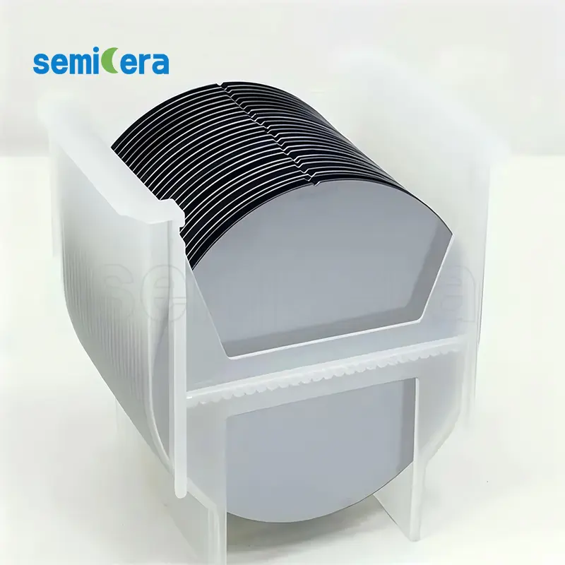
Semicera introduces the Wafer Cassette Carrier, a critical solution for the secure and efficient handling of semiconductor wafers. This carrier is engineered to meet the stringent requirements of the semiconductor industry, ensuring the protection and integrity of your wafers throughout the manufacturing process.
Caratteristiche chiave:
• Robust Construction: IL Wafer Cassette Carrier is built from high-quality, durable materials that withstand the rigors of semiconductor environments, providing reliable protection against contamination and physical damage.
• Precise Alignment: Designed for precise wafer alignment, this carrier ensures that wafers are securely held in place, minimizing the risk of misalignment or damage during transport.
• Easy Handling: Ergonomically designed for ease of use, the carrier simplifies the loading and unloading process, improving workflow efficiency in cleanroom environments.
• Compatibility: Compatible with a wide range of wafer sizes and types, making it versatile for various semiconductor manufacturing needs.
Experience unparalleled protection and convenience with Semicera’s Wafer Cassette Carrier. Our carrier is designed to meet the highest standards of semiconductor manufacturing, ensuring your wafers remain in pristine condition from start to finish. Trust Semicera to deliver the quality and reliability you need for your most critical processes.
|
Elementi |
Produzione |
Ricerca |
Manichino |
|
Parametri cristallini |
|||
|
Politipo |
4H |
||
|
Errore di orientamento della superficie |
4±0.15° |
||
|
Parametri elettrici |
|||
|
Drogante |
azoto di tipo n |
||
|
Resistività |
0,015-0,025ohm · cm |
||
|
Parametri meccanici |
|||
|
Diametro |
150,0 ± 0,2 mm |
||
|
Spessore |
350 ± 25 µm |
||
|
Orientamento piatto primario |
[1-100]±5° |
||
|
Lunghezza piatta primaria |
47,5 ± 1,5 mm |
||
|
Piatto secondario |
Nessuno |
||
|
TTV |
≤5 µm |
≤10 µm |
≤15 µm |
|
LTV |
≤3 μm (5mm*5mm) |
≤5 μm (5 mm*5 mm) |
≤10 μm (5 mm*5 mm) |
|
Arco |
-15μm ~ 15μm |
-35μm ~ 35 μm |
-45μm ~ 45μm |
|
Ordito |
≤35 µm |
≤45 µm |
≤55 µm |
|
Front (Si-Face) Rughess (AFM) |
RA≤0,2 nm (5μm*5μm) |
||
|
Struttura |
|||
|
Densità di micrivipe |
<1 ea/cm2 |
<10 ea/cm2 |
<15 ea/cm2 |
|
Impurità dei metalli |
≤5E10atoms/cm2 |
N / A |
|
|
BPD |
≤1500 ea/cm2 |
≤3000 ea/cm2 |
N / A |
|
TSD |
≤500 ea/cm2 |
≤1000 ea/cm2 |
N / A |
|
Qualità anteriore |
|||
|
Davanti |
Si |
||
|
Finitura superficiale |
Si-Face CMP |
||
|
Particelle |
≤60ea/wafer (dimensione≥0,3μm) |
N / A |
|
|
Graffi |
≤5ea/mm. Lunghezza cumulativa ≤Diameter |
Diametro cumulativo della lunghezza ≤2* |
N / A |
|
Buccia/pozzi/macchie/striature/crepe/contaminazione |
Nessuno |
N / A |
|
|
Bordo chips/riendi/frattura/piastre esadecimale |
Nessuno |
||
|
Aree politepi |
Nessuno |
Area cumulativa≤20% |
Area cumulativa≤30% |
|
Marcatura laser anteriore |
Nessuno |
||
|
Qualità alla schiena |
|||
|
Finitura posteriore |
C-FACE CMP |
||
|
Graffi |
≤5ea/mm, lunghezza cumulativa≤2*diametro |
N / A |
|
|
Difetti posteriori (bordo chip/rientri) |
Nessuno |
||
|
Rugosità posteriore |
RA≤0,2 nm (5μm*5μm) |
||
|
Marcatura laser sul retro |
1 mm (dal bordo superiore) |
||
|
Bordo |
|||
|
Bordo |
Smussare |
||
|
Confezione |
|||
|
Confezione |
Prepasto EPI con imballaggio a vuoto Packaging a cassette multi-wafer |
||
|
*Note : “NA” significa che nessuna richiesta di richiesta non menzionata può fare riferimento a semi-std. |
|||


