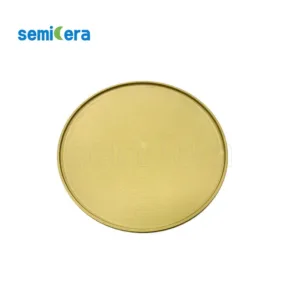
Semicera’s Silicon Carbide Epitaxy is engineered to meet the rigorous demands of modern semiconductor applications. By utilizing advanced epitaxial growth techniques, we ensure that each silicon carbide layer exhibits exceptional crystalline quality, uniformity, and minimal defect density. These characteristics are crucial for developing high-performance power electronics, where efficiency and thermal management are paramount.
The Silicon Carbide Epitaxy process at Semicera is optimized to produce epitaxial layers with precise thickness and doping control, ensuring consistent performance across a range of devices. This level of precision is essential for applications in electric vehicles, renewable energy systems, and high-frequency communications, where reliability and efficiency are critical.
Moreover, Semicera’s Silicon Carbide Epitaxy offers enhanced thermal conductivity and higher breakdown voltage, making it the preferred choice for devices that operate under extreme conditions. These properties contribute to longer device lifetimes and improved overall system efficiency, particularly in high-power and high-temperature environments.
Semicera also provides customization options for Silicon Carbide Epitaxy, allowing for tailored solutions that meet specific device requirements. Whether for research or large-scale production, our epitaxial layers are designed to support the next generation of semiconductor innovations, enabling the development of more powerful, efficient, and reliable electronic devices.
By integrating cutting-edge technology and stringent quality control processes, Semicera ensures that our Silicon Carbide Epitaxy products not only meet but exceed industry standards. This commitment to excellence makes our epitaxial layers the ideal foundation for advanced semiconductor applications, paving the way for breakthroughs in power electronics and optoelectronics.
|
アイテム |
生産 |
研究 |
ダミー |
|
クリスタルパラメーター |
|||
|
ポリタイプ |
4H |
||
|
表面向きエラー |
4±0.15° |
||
|
電気パラメーター |
|||
|
ドーパント |
N型窒素 |
||
|
抵抗率 |
0.015-0.025OHM・CM |
||
|
機械的パラメーター |
|||
|
直径 |
150.0±0.2mm |
||
|
厚さ |
350±25 µm |
||
|
一次フラットオリエンテーション |
[1-100]±5° |
||
|
プライマリフラット長 |
47.5±1.5mm |
||
|
二次フラット |
なし |
||
|
TTV |
≤5 µm |
≤10 µm |
≤15 µm |
|
LTV |
≤3μm(5mm*5mm) |
≤5μm(5mm*5mm) |
≤10μm(5mm*5mm) |
|
弓 |
-15μm〜15μm |
-35μm〜35μm |
-45μm〜45μm |
|
ワープ |
≤35 µm |
≤45 µm |
≤55 µm |
|
フロント(si-face)粗さ(AFM) |
RA≤0.2nm(5μm*5μm) |
||
|
構造 |
|||
|
マイクロパイプ密度 |
<1 EA/CM2 |
<10 EA/CM2 |
<15 EA/CM2 |
|
金属の不純物 |
≤5E10atoms/cm2 |
Na |
|
|
BPD |
≤1500 EA/CM2 |
≤3000 EA/CM2 |
Na |
|
TSD |
≤500 EA/CM2 |
≤1000 EA/CM2 |
Na |
|
フロント品質 |
|||
|
フロント |
si |
||
|
表面仕上げ |
SI-FACE CMP |
||
|
粒子 |
≤60EA/ウェーハ(サイズ以上0.3μm) |
Na |
|
|
傷 |
≤5EA/mm。累積長さ≤diameter |
累積長さ2*直径 |
Na |
|
オレンジの皮/ピット/染色/縞/亀裂/汚染 |
なし |
Na |
|
|
エッジチップ/インデント/骨折/ヘックスプレート |
なし |
||
|
ポリタイプの領域 |
なし |
累積面積≤20% |
累積面積以下30% |
|
フロントレーザーマーキング |
なし |
||
|
バック品質 |
|||
|
バックフィニッシュ |
C-Face CMP |
||
|
傷 |
≤5EA/mm、累積長さ2*直径 |
Na |
|
|
バック欠陥(エッジチップ/インデント) |
なし |
||
|
背中の粗さ |
RA≤0.2nm(5μm*5μm) |
||
|
バックレーザーマーキング |
1 mm(上端から) |
||
|
角 |
|||
|
角 |
面取り |
||
|
パッケージング |
|||
|
パッケージング |
真空パッケージングを使用したEPIの準備 マルチワーファーカセットパッケージ |
||
|
*注:「NA」とは、言及されていないリクエスト項目がSemi-STDを参照することはできないことを意味します。 |
|||