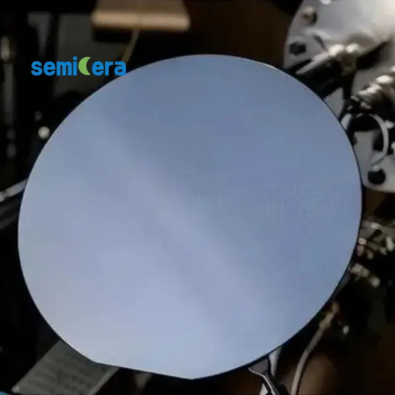
セミセラ 誇らしげに申し出ます ga2O3 エピタキシー、パワーエレクトロニクスとオプトエレクトロニクスの境界を押し上げるように設計された最先端のソリューション。この高度なエピタキシャル技術は、酸化ガリウムのユニークな特性を活用しています(GA2O3)要求の厳しいアプリケーションで優れたパフォーマンスを提供する。
重要な機能:
• 例外的なワイドバンドギャップ: ga2O3 エピタキシー 超幅のバンドギャップを備えており、高電力環境でのブレークダウン電圧と効率的な動作を可能にします。
• 高い熱伝導率: エピタキシャル層は優れた熱伝導率を提供し、高温条件下でも安定した動作を確保し、高周波デバイスに最適です。
• 優れた材料品質: 特にパワートランジスタやUV検出器などの重要なアプリケーションで、最小限の欠陥で高い結晶品質を達成し、最適なデバイスのパフォーマンスと寿命を確保します。
• アプリケーションの汎用性: Power Electronics、RFアプリケーション、およびOptoElectronicsに最適であり、次世代半導体デバイスの信頼できる基盤を提供します。
の可能性を発見してください ga2O3 エピタキシー Semiceraの革新的なソリューションを使用しています。当社のエピタキシャル製品は、品質とパフォーマンスの最高水準を満たすように設計されており、デバイスが最大の効率と信頼性で動作できるようにします。最先端の半導体テクノロジーについては、Semiceraを選択してください。
|
アイテム |
生産 |
研究 |
ダミー |
|
クリスタルパラメーター |
|||
|
ポリタイプ |
4H |
||
|
表面向きエラー |
4±0.15° |
||
|
電気パラメーター |
|||
|
ドーパント |
N型窒素 |
||
|
抵抗率 |
0.015-0.025OHM・CM |
||
|
機械的パラメーター |
|||
|
直径 |
150.0±0.2mm |
||
|
厚さ |
350±25 µm |
||
|
一次フラットオリエンテーション |
[1-100]±5° |
||
|
プライマリフラット長 |
47.5±1.5mm |
||
|
二次フラット |
なし |
||
|
TTV |
≤5 µm |
≤10 µm |
≤15 µm |
|
LTV |
≤3μm(5mm*5mm) |
≤5μm(5mm*5mm) |
≤10μm(5mm*5mm) |
|
弓 |
-15μm〜15μm |
-35μm〜35μm |
-45μm〜45μm |
|
ワープ |
≤35 µm |
≤45 µm |
≤55 µm |
|
フロント(si-face)粗さ(AFM) |
RA≤0.2nm(5μm*5μm) |
||
|
構造 |
|||
|
マイクロパイプ密度 |
<1 EA/CM2 |
<10 EA/CM2 |
<15 EA/CM2 |
|
金属の不純物 |
≤5E10atoms/cm2 |
Na |
|
|
BPD |
≤1500 EA/CM2 |
≤3000 EA/CM2 |
Na |
|
TSD |
≤500 EA/CM2 |
≤1000 EA/CM2 |
Na |
|
フロント品質 |
|||
|
フロント |
si |
||
|
表面仕上げ |
SI-FACE CMP |
||
|
粒子 |
≤60EA/ウェーハ(サイズ以上0.3μm) |
Na |
|
|
傷 |
≤5EA/mm。累積長さ≤diameter |
累積長さ2*直径 |
Na |
|
オレンジの皮/ピット/染色/縞/亀裂/汚染 |
なし |
Na |
|
|
エッジチップ/インデント/骨折/ヘックスプレート |
なし |
||
|
ポリタイプの領域 |
なし |
累積面積≤20% |
累積面積以下30% |
|
フロントレーザーマーキング |
なし |
||
|
バック品質 |
|||
|
バックフィニッシュ |
C-Face CMP |
||
|
傷 |
≤5EA/mm、累積長さ2*直径 |
Na |
|
|
バック欠陥(エッジチップ/インデント) |
なし |
||
|
背中の粗さ |
RA≤0.2nm(5μm*5μm) |
||
|
バックレーザーマーキング |
1 mm(上端から) |
||
|
角 |
|||
|
角 |
面取り |
||
|
パッケージング |
|||
|
パッケージング |
真空パッケージングを使用したEPIの準備 マルチワーファーカセットパッケージ |
||
|
*注:「NA」とは、言及されていないリクエスト項目がSemi-STDを参照することはできないことを意味します。 |
|||


