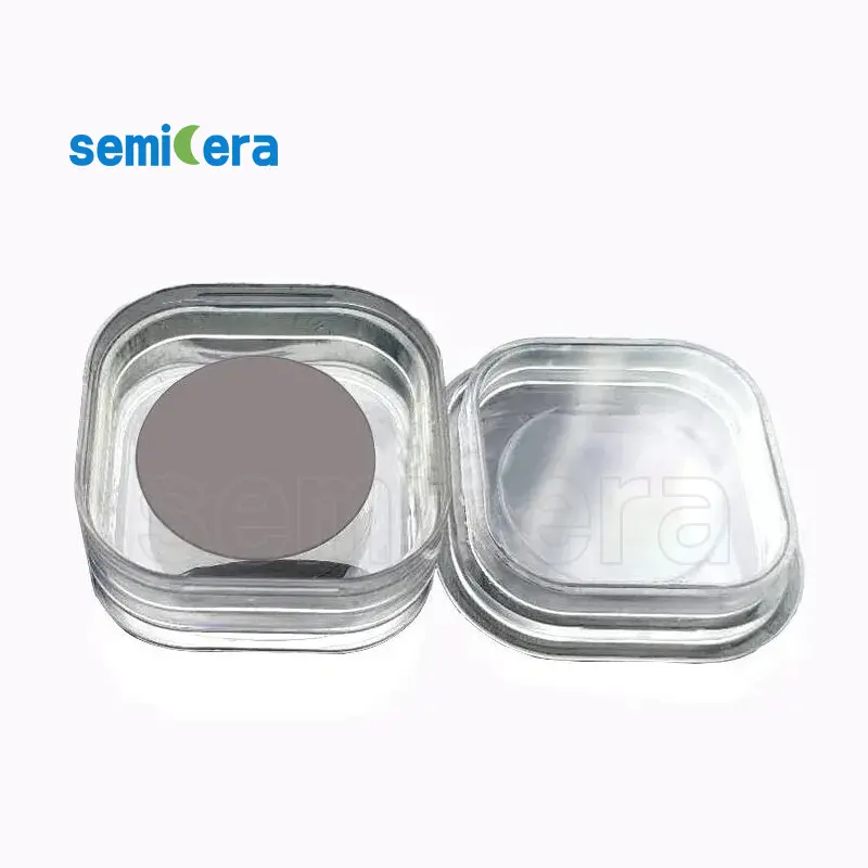
セミセラ 提示することを誇りに思っています 30mm硝化アルミニウムウェーハ基板、最新の電子および光電子アプリケーションの厳しい需要を満たすために設計された一流の材料。窒化アルミニウム(ALN)基質は、優れた熱伝導率と電気断熱特性で有名であり、高性能デバイスに理想的な選択肢となっています。
重要な機能:
• 例外的な熱伝導率: 30mm硝化アルミニウムウェーハ基板 最大170 W/MKの熱伝導率を誇り、他の基質材料よりも大幅に高く、高出力用途での効率的な熱散逸を確保しています。
• 高い電気断熱: 優れた電気断熱特性により、この基板はクロストークと信号干渉を最小限に抑え、RFおよびマイクロ波アプリケーションに最適です。
• 機械的強度: 30mm硝化アルミニウムウェーハ基板 優れた機械的強度と安定性を提供し、厳密な動作条件下でも耐久性と信頼性を確保します。
• 汎用性の高いアプリケーション: この基板は、高出力LED、レーザーダイオード、RFコンポーネントでの使用に最適であり、最も要求の厳しいプロジェクトに堅牢で信頼できる基盤を提供します。
• 精密製造: Semiceraは、各ウェーハ基板が最高の精度で製造されることを保証し、高度な電子デバイスの厳密な基準を満たすために均一な厚さと表面品質を提供します。
セミセラを使用してデバイスの効率と信頼性を最大化する 30mm硝化アルミニウムウェーハ基板。当社の基板は、優れた性能を提供するように設計されており、電子および光電子システムが最高の動作をするようにします。品質と革新において業界を導く最先端の資料のセミセラを信頼してください。
|
アイテム |
生産 |
研究 |
ダミー |
|
クリスタルパラメーター |
|||
|
ポリタイプ |
4H |
||
|
表面向きエラー |
4±0.15° |
||
|
電気パラメーター |
|||
|
ドーパント |
N型窒素 |
||
|
抵抗率 |
0.015-0.025OHM・CM |
||
|
機械的パラメーター |
|||
|
直径 |
150.0±0.2mm |
||
|
厚さ |
350±25 µm |
||
|
一次フラットオリエンテーション |
[1-100]±5° |
||
|
プライマリフラット長 |
47.5±1.5mm |
||
|
二次フラット |
なし |
||
|
TTV |
≤5 µm |
≤10 µm |
≤15 µm |
|
LTV |
≤3μm(5mm*5mm) |
≤5μm(5mm*5mm) |
≤10μm(5mm*5mm) |
|
弓 |
-15μm〜15μm |
-35μm〜35μm |
-45μm〜45μm |
|
ワープ |
≤35 µm |
≤45 µm |
≤55 µm |
|
フロント(si-face)粗さ(AFM) |
RA≤0.2nm(5μm*5μm) |
||
|
構造 |
|||
|
マイクロパイプ密度 |
<1 EA/CM2 |
<10 EA/CM2 |
<15 EA/CM2 |
|
金属の不純物 |
≤5E10atoms/cm2 |
Na |
|
|
BPD |
≤1500 EA/CM2 |
≤3000 EA/CM2 |
Na |
|
TSD |
≤500 EA/CM2 |
≤1000 EA/CM2 |
Na |
|
フロント品質 |
|||
|
フロント |
si |
||
|
表面仕上げ |
SI-FACE CMP |
||
|
粒子 |
≤60EA/ウェーハ(サイズ以上0.3μm) |
Na |
|
|
傷 |
≤5EA/mm。累積長さ≤diameter |
累積長さ2*直径 |
Na |
|
オレンジの皮/ピット/染色/縞/亀裂/汚染 |
なし |
Na |
|
|
エッジチップ/インデント/骨折/ヘックスプレート |
なし |
||
|
ポリタイプの領域 |
なし |
累積面積≤20% |
累積面積以下30% |
|
フロントレーザーマーキング |
なし |
||
|
バック品質 |
|||
|
バックフィニッシュ |
C-Face CMP |
||
|
傷 |
≤5EA/mm、累積長さ2*直径 |
Na |
|
|
バック欠陥(エッジチップ/インデント) |
なし |
||
|
背中の粗さ |
RA≤0.2nm(5μm*5μm) |
||
|
バックレーザーマーキング |
1 mm(上端から) |
||
|
角 |
|||
|
角 |
面取り |
||
|
パッケージング |
|||
|
パッケージング |
真空パッケージングを使用したEPIの準備 マルチワーファーカセットパッケージ |
||
|
*注:「NA」とは、言及されていないリクエスト項目がSemi-STDを参照することはできないことを意味します。 |
|||


