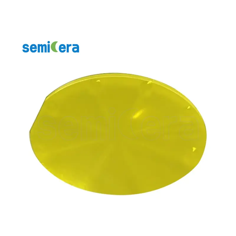
Semicera 3C-SiC Wafer Substrates are engineered to provide a robust platform for next-generation power electronics and high-frequency devices. With superior thermal properties and electrical characteristics, these substrates are designed to meet the demanding requirements of modern technology.
The 3C-SiC (Cubic Silicon Carbide) structure of Semicera Wafer Substrates offers unique advantages, including higher thermal conductivity and a lower thermal expansion coefficient compared to other semiconductor materials. This makes them an excellent choice for devices operating under extreme temperatures and high-power conditions.
With a high electrical breakdown voltage and superior chemical stability, Semicera 3C-SiC Wafer Substrates ensure long-lasting performance and reliability. These properties are critical for applications such as high-frequency radar, solid-state lighting, and power inverters, where efficiency and durability are paramount.
Semicera’s commitment to quality is reflected in the meticulous manufacturing process of their 3C-SiC Wafer Substrates, ensuring uniformity and consistency across every batch. This precision contributes to the overall performance and longevity of the electronic devices built upon them.
By choosing Semicera 3C-SiC Wafer Substrates, manufacturers gain access to a cutting-edge material that enables the development of smaller, faster, and more efficient electronic components. Semicera continues to support technological innovation by providing reliable solutions that meet the evolving demands of the semiconductor industry.
|
アイテム |
生産 |
研究 |
ダミー |
|
クリスタルパラメーター |
|||
|
ポリタイプ |
4H |
||
|
表面向きエラー |
4±0.15° |
||
|
電気パラメーター |
|||
|
ドーパント |
N型窒素 |
||
|
抵抗率 |
0.015-0.025OHM・CM |
||
|
機械的パラメーター |
|||
|
直径 |
150.0±0.2mm |
||
|
厚さ |
350±25 µm |
||
|
一次フラットオリエンテーション |
[1-100]±5° |
||
|
プライマリフラット長 |
47.5±1.5mm |
||
|
二次フラット |
なし |
||
|
TTV |
≤5 µm |
≤10 µm |
≤15 µm |
|
LTV |
≤3μm(5mm*5mm) |
≤5μm(5mm*5mm) |
≤10μm(5mm*5mm) |
|
弓 |
-15μm〜15μm |
-35μm〜35μm |
-45μm〜45μm |
|
ワープ |
≤35 µm |
≤45 µm |
≤55 µm |
|
フロント(si-face)粗さ(AFM) |
RA≤0.2nm(5μm*5μm) |
||
|
構造 |
|||
|
マイクロパイプ密度 |
<1 EA/CM2 |
<10 EA/CM2 |
<15 EA/CM2 |
|
金属の不純物 |
≤5E10atoms/cm2 |
Na |
|
|
BPD |
≤1500 EA/CM2 |
≤3000 EA/CM2 |
Na |
|
TSD |
≤500 EA/CM2 |
≤1000 EA/CM2 |
Na |
|
フロント品質 |
|||
|
フロント |
si |
||
|
表面仕上げ |
SI-FACE CMP |
||
|
粒子 |
≤60EA/ウェーハ(サイズ以上0.3μm) |
Na |
|
|
傷 |
≤5EA/mm。累積長さ≤diameter |
累積長さ2*直径 |
Na |
|
オレンジの皮/ピット/染色/縞/亀裂/汚染 |
なし |
Na |
|
|
エッジチップ/インデント/骨折/ヘックスプレート |
なし |
||
|
ポリタイプの領域 |
なし |
累積面積≤20% |
累積面積以下30% |
|
フロントレーザーマーキング |
なし |
||
|
バック品質 |
|||
|
バックフィニッシュ |
C-Face CMP |
||
|
傷 |
≤5EA/mm、累積長さ2*直径 |
Na |
|
|
バック欠陥(エッジチップ/インデント) |
なし |
||
|
背中の粗さ |
RA≤0.2nm(5μm*5μm) |
||
|
バックレーザーマーキング |
1 mm(上端から) |
||
|
角 |
|||
|
角 |
面取り |
||
|
パッケージング |
|||
|
パッケージング |
真空パッケージングを使用したEPIの準備 マルチワーファーカセットパッケージ |
||
|
*注:「NA」とは、言及されていないリクエスト項目がSemi-STDを参照することはできないことを意味します。 |
|||


