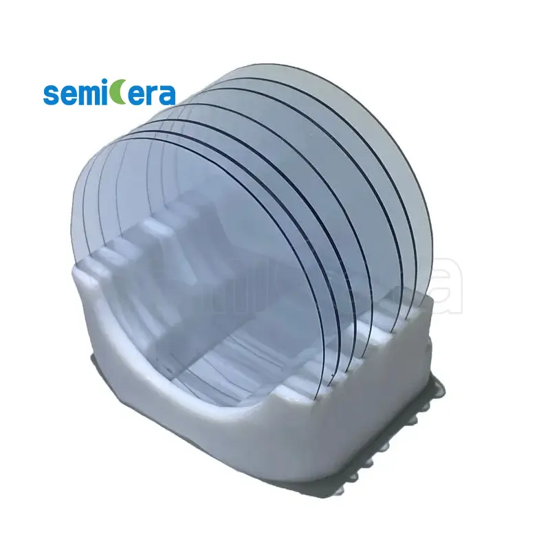
セミセラ proudly introduces its 4″ Gallium Oxide Substrates, a groundbreaking material engineered to meet the growing demands of high-performance semiconductor devices. Gallium Oxide (Ga2O3) substrates offer an ultra-wide bandgap, making them ideal for next-generation power electronics, UV optoelectronics, and high-frequency devices.
重要な機能:
• Ultra-Wide Bandgap: 4″ Gallium Oxide Substrates boast a bandgap of approximately 4.8 eV, allowing for exceptional voltage and temperature tolerance, significantly outperforming traditional semiconductor materials like silicon.
• High Breakdown Voltage: These substrates enable devices to operate at higher voltages and powers, making them perfect for high-voltage applications in power electronics.
• Superior Thermal Stability: Gallium Oxide substrates offer excellent thermal conductivity, ensuring stable performance under extreme conditions, ideal for use in demanding environments.
• High Material Quality: With low defect densities and high crystal quality, these substrates ensure reliable and consistent performance, enhancing the efficiency and durability of your devices.
• Versatile Application: Suitable for a wide range of applications, including power transistors, Schottky diodes, and UV-C LED devices, enabling innovations in both power and optoelectronic fields.
Explore the future of semiconductor technology with Semicera’s 4″ Gallium Oxide Substrates. Our substrates are designed to support the most advanced applications, providing the reliability and efficiency required for today’s cutting-edge devices. Trust Semicera for quality and innovation in your semiconductor materials.
|
アイテム |
生産 |
研究 |
ダミー |
|
クリスタルパラメーター |
|||
|
ポリタイプ |
4H |
||
|
表面向きエラー |
4±0.15° |
||
|
電気パラメーター |
|||
|
ドーパント |
N型窒素 |
||
|
抵抗率 |
0.015-0.025OHM・CM |
||
|
機械的パラメーター |
|||
|
直径 |
150.0±0.2mm |
||
|
厚さ |
350±25 µm |
||
|
一次フラットオリエンテーション |
[1-100]±5° |
||
|
プライマリフラット長 |
47.5±1.5mm |
||
|
二次フラット |
なし |
||
|
TTV |
≤5 µm |
≤10 µm |
≤15 µm |
|
LTV |
≤3μm(5mm*5mm) |
≤5μm(5mm*5mm) |
≤10μm(5mm*5mm) |
|
弓 |
-15μm〜15μm |
-35μm〜35μm |
-45μm〜45μm |
|
ワープ |
≤35 µm |
≤45 µm |
≤55 µm |
|
フロント(si-face)粗さ(AFM) |
RA≤0.2nm(5μm*5μm) |
||
|
構造 |
|||
|
マイクロパイプ密度 |
<1 EA/CM2 |
<10 EA/CM2 |
<15 EA/CM2 |
|
金属の不純物 |
≤5E10atoms/cm2 |
Na |
|
|
BPD |
≤1500 EA/CM2 |
≤3000 EA/CM2 |
Na |
|
TSD |
≤500 EA/CM2 |
≤1000 EA/CM2 |
Na |
|
フロント品質 |
|||
|
フロント |
si |
||
|
表面仕上げ |
SI-FACE CMP |
||
|
粒子 |
≤60EA/ウェーハ(サイズ以上0.3μm) |
Na |
|
|
傷 |
≤5EA/mm。累積長さ≤diameter |
累積長さ2*直径 |
Na |
|
オレンジの皮/ピット/染色/縞/亀裂/汚染 |
なし |
Na |
|
|
エッジチップ/インデント/骨折/ヘックスプレート |
なし |
||
|
ポリタイプの領域 |
なし |
累積面積≤20% |
累積面積以下30% |
|
フロントレーザーマーキング |
なし |
||
|
バック品質 |
|||
|
バックフィニッシュ |
C-Face CMP |
||
|
傷 |
≤5EA/mm、累積長さ2*直径 |
Na |
|
|
バック欠陥(エッジチップ/インデント) |
なし |
||
|
背中の粗さ |
RA≤0.2nm(5μm*5μm) |
||
|
バックレーザーマーキング |
1 mm(上端から) |
||
|
角 |
|||
|
角 |
面取り |
||
|
パッケージング |
|||
|
パッケージング |
真空パッケージングを使用したEPIの準備 マルチワーファーカセットパッケージ |
||
|
*注:「NA」とは、言及されていないリクエスト項目がSemi-STDを参照することはできないことを意味します。 |
|||


