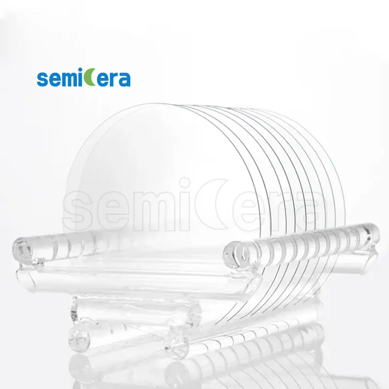
Semicera’s 4 Inch High Purity Semi-Insulating (HPSI) SiC Double-side Polished Wafer Substrates are crafted to meet the exacting demands of the semiconductor industry. These substrates are designed with exceptional flatness and purity, offering an optimal platform for cutting-edge electronic devices.
These HPSI SiC wafers are distinguished by their superior thermal conductivity and electrical insulation properties, making them an excellent choice for high-frequency and high-power applications. The double-side polishing process ensures minimal surface roughness, which is crucial for enhancing device performance and longevity.
The high purity of Semicera’s SiC wafers minimizes defects and impurities, leading to higher yield rates and device reliability. These substrates are suitable for a wide range of applications, including microwave devices, power electronics, and LED technologies, where precision and durability are essential.
With a focus on innovation and quality, Semicera utilizes advanced manufacturing techniques to produce wafers that meet the stringent requirements of modern electronics. The double-sided polishing not only improves the mechanical strength but also facilitates better integration with other semiconductor materials.
By choosing Semicera’s 4 Inch High Purity Semi-Insulating HPSI SiC Double-side Polished Wafer Substrates, manufacturers can leverage the benefits of enhanced thermal management and electrical insulation, paving the way for the development of more efficient and powerful electronic devices. Semicera continues to lead the industry with its commitment to quality and technological advancement.
|
アイテム |
生産 |
研究 |
ダミー |
|
クリスタルパラメーター |
|||
|
ポリタイプ |
4H |
||
|
表面向きエラー |
4±0.15° |
||
|
電気パラメーター |
|||
|
ドーパント |
N型窒素 |
||
|
抵抗率 |
0.015-0.025OHM・CM |
||
|
機械的パラメーター |
|||
|
直径 |
150.0±0.2mm |
||
|
厚さ |
350±25 µm |
||
|
一次フラットオリエンテーション |
[1-100]±5° |
||
|
プライマリフラット長 |
47.5±1.5mm |
||
|
二次フラット |
なし |
||
|
TTV |
≤5 µm |
≤10 µm |
≤15 µm |
|
LTV |
≤3μm(5mm*5mm) |
≤5μm(5mm*5mm) |
≤10μm(5mm*5mm) |
|
弓 |
-15μm〜15μm |
-35μm〜35μm |
-45μm〜45μm |
|
ワープ |
≤35 µm |
≤45 µm |
≤55 µm |
|
フロント(si-face)粗さ(AFM) |
RA≤0.2nm(5μm*5μm) |
||
|
構造 |
|||
|
マイクロパイプ密度 |
<1 EA/CM2 |
<10 EA/CM2 |
<15 EA/CM2 |
|
金属の不純物 |
≤5E10atoms/cm2 |
Na |
|
|
BPD |
≤1500 EA/CM2 |
≤3000 EA/CM2 |
Na |
|
TSD |
≤500 EA/CM2 |
≤1000 EA/CM2 |
Na |
|
フロント品質 |
|||
|
フロント |
si |
||
|
表面仕上げ |
SI-FACE CMP |
||
|
粒子 |
≤60EA/ウェーハ(サイズ以上0.3μm) |
Na |
|
|
傷 |
≤5EA/mm。累積長さ≤diameter |
累積長さ2*直径 |
Na |
|
オレンジの皮/ピット/染色/縞/亀裂/汚染 |
なし |
Na |
|
|
エッジチップ/インデント/骨折/ヘックスプレート |
なし |
||
|
ポリタイプの領域 |
なし |
累積面積≤20% |
累積面積以下30% |
|
フロントレーザーマーキング |
なし |
||
|
バック品質 |
|||
|
バックフィニッシュ |
C-Face CMP |
||
|
傷 |
≤5EA/mm、累積長さ2*直径 |
Na |
|
|
バック欠陥(エッジチップ/インデント) |
なし |
||
|
背中の粗さ |
RA≤0.2nm(5μm*5μm) |
||
|
バックレーザーマーキング |
1 mm(上端から) |
||
|
角 |
|||
|
角 |
面取り |
||
|
パッケージング |
|||
|
パッケージング |
真空パッケージングを使用したEPIの準備 マルチワーファーカセットパッケージ |
||
|
*注:「NA」とは、言及されていないリクエスト項目がSemi-STDを参照することはできないことを意味します。 |
|||


