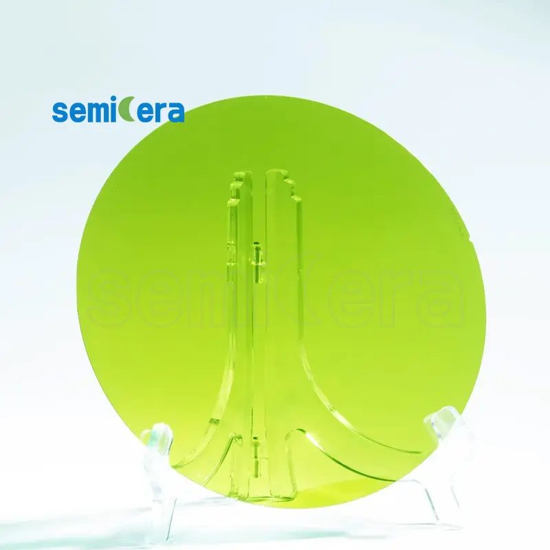
Semicera’s 4 Inch N-type SiC Substrates are crafted to meet the exacting standards of the semiconductor industry. These substrates provide a high-performance foundation for a wide range of electronic applications, offering exceptional conductivity and thermal properties.
The N-type doping of these SiC substrates enhances their electrical conductivity, making them particularly suitable for high-power and high-frequency applications. This property allows for the efficient operation of devices such as diodes, transistors, and amplifiers, where minimizing energy loss is crucial.
Semicera utilizes state-of-the-art manufacturing processes to ensure that each substrate exhibits excellent surface quality and uniformity. This precision is critical for applications in power electronics, microwave devices, and other technologies that demand reliable performance under extreme conditions.
Incorporating Semicera’s N-type SiC substrates into your production line means benefiting from materials that offer superior heat dissipation and electrical stability. These substrates are ideal for creating components that require durability and efficiency, such as power conversion systems and RF amplifiers.
By choosing Semicera’s 4 Inch N-type SiC Substrates, you are investing in a product that combines innovative material science with meticulous craftsmanship. Semicera continues to lead the industry by providing solutions that support the development of cutting-edge semiconductor technologies, ensuring high performance and reliability.
|
アイテム |
生産 |
研究 |
ダミー |
|
クリスタルパラメーター |
|||
|
ポリタイプ |
4H |
||
|
表面向きエラー |
4±0.15° |
||
|
電気パラメーター |
|||
|
ドーパント |
N型窒素 |
||
|
抵抗率 |
0.015-0.025OHM・CM |
||
|
機械的パラメーター |
|||
|
直径 |
150.0±0.2mm |
||
|
厚さ |
350±25 µm |
||
|
一次フラットオリエンテーション |
[1-100]±5° |
||
|
プライマリフラット長 |
47.5±1.5mm |
||
|
二次フラット |
なし |
||
|
TTV |
≤5 µm |
≤10 µm |
≤15 µm |
|
LTV |
≤3μm(5mm*5mm) |
≤5μm(5mm*5mm) |
≤10μm(5mm*5mm) |
|
弓 |
-15μm〜15μm |
-35μm〜35μm |
-45μm〜45μm |
|
ワープ |
≤35 µm |
≤45 µm |
≤55 µm |
|
フロント(si-face)粗さ(AFM) |
RA≤0.2nm(5μm*5μm) |
||
|
構造 |
|||
|
マイクロパイプ密度 |
<1 EA/CM2 |
<10 EA/CM2 |
<15 EA/CM2 |
|
金属の不純物 |
≤5E10atoms/cm2 |
Na |
|
|
BPD |
≤1500 EA/CM2 |
≤3000 EA/CM2 |
Na |
|
TSD |
≤500 EA/CM2 |
≤1000 EA/CM2 |
Na |
|
フロント品質 |
|||
|
フロント |
si |
||
|
表面仕上げ |
SI-FACE CMP |
||
|
粒子 |
≤60EA/ウェーハ(サイズ以上0.3μm) |
Na |
|
|
傷 |
≤5EA/mm。累積長さ≤diameter |
累積長さ2*直径 |
Na |
|
オレンジの皮/ピット/染色/縞/亀裂/汚染 |
なし |
Na |
|
|
エッジチップ/インデント/骨折/ヘックスプレート |
なし |
||
|
ポリタイプの領域 |
なし |
累積面積≤20% |
累積面積以下30% |
|
フロントレーザーマーキング |
なし |
||
|
バック品質 |
|||
|
バックフィニッシュ |
C-Face CMP |
||
|
傷 |
≤5EA/mm、累積長さ2*直径 |
Na |
|
|
バック欠陥(エッジチップ/インデント) |
なし |
||
|
背中の粗さ |
RA≤0.2nm(5μm*5μm) |
||
|
バックレーザーマーキング |
1 mm(上端から) |
||
|
角 |
|||
|
角 |
面取り |
||
|
パッケージング |
|||
|
パッケージング |
真空パッケージングを使用したEPIの準備 マルチワーファーカセットパッケージ |
||
|
*注:「NA」とは、言及されていないリクエスト項目がSemi-STDを参照することはできないことを意味します。 |
|||


