Silicon carbide (SiC) single crystal material has a large band gap width (~Si 3 times), high thermal conductivity (~Si 3.3 times or GaAs 10 times), high electron saturation migration rate (~Si 2.5 times), high breakdown electric field (~Si 10 times or GaAs 5 times) and other outstanding characteristics.
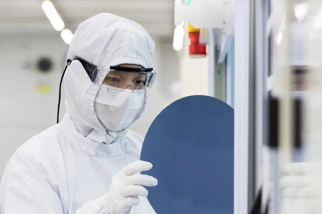
Semicera energy can provide customers with high-quality Conductive (Conductive), Semi-insulating (Semi-insulating), HPSI (High Purity semi-insulating) silicon carbide substrate; In addition, we can provide customers with homogeneous and heterogeneous silicon carbide epitaxial sheets; We can also customize the epitaxial sheet according to the specific needs of customers, and there is no minimum order quantity.
|
アイテム |
生産 |
研究 |
ダミー |
|
クリスタルパラメーター |
|||
|
ポリタイプ |
4H |
||
|
表面向きエラー |
<11-20 >4±0.15° |
||
|
電気パラメーター |
|||
|
ドーパント |
N型窒素 |
||
|
抵抗率 |
0.015-0.025ohm·cm |
||
|
機械的パラメーター |
|||
|
直径 |
99.5 – 100mm |
||
|
厚さ |
350±25 μm |
||
|
一次フラットオリエンテーション |
[1-100]±5° |
||
|
プライマリフラット長 |
32.5±1.5mm |
||
|
Secondary flat position |
90° CW from primary flat ±5°. silicon face up |
||
|
Secondary flat length |
18±1.5mm |
||
|
TTV |
≤5 μm |
≤10 μm |
≤20 μm |
|
LTV |
≤2 μm(5mm*5mm) |
≤5 μm(5mm*5mm) |
Na |
|
弓 |
-15μm ~ 15μm |
-35μm ~ 35μm |
-45μm ~ 45μm |
|
ワープ |
≤20 μm |
≤45 μm |
≤50 μm |
|
フロント(si-face)粗さ(AFM) |
Ra≤0.2nm (5μm*5μm) |
||
|
構造 |
|||
|
マイクロパイプ密度 |
≤1 ea/cm2 |
≤5 ea/cm2 |
≤10 ea/cm2 |
|
金属の不純物 |
≤5E10atoms/cm2 |
Na |
|
|
BPD |
≤1500 ea/cm2 |
≤3000 ea/cm2 |
Na |
|
TSD |
≤500 ea/cm2 |
≤1000 ea/cm2 |
Na |
|
フロント品質 |
|||
|
フロント |
si |
||
|
表面仕上げ |
SI-FACE CMP |
||
|
粒子 |
≤60ea/wafer (size≥0.3μm) |
Na |
|
|
傷 |
≤2ea/mm. Cumulative length ≤Diameter |
Cumulative length≤2*Diameter |
Na |
|
オレンジの皮/ピット/染色/縞/亀裂/汚染 |
なし |
Na |
|
|
エッジチップ/インデント/骨折/ヘックスプレート |
なし |
Na |
|
|
ポリタイプの領域 |
なし |
Cumulative area≤20% |
Cumulative area≤30% |
|
フロントレーザーマーキング |
なし |
||
|
バック品質 |
|||
|
バックフィニッシュ |
C-Face CMP |
||
|
傷 |
≤5ea/mm,Cumulative length≤2*Diameter |
Na |
|
|
バック欠陥(エッジチップ/インデント) |
なし |
||
|
背中の粗さ |
Ra≤0.2nm (5μm*5μm) |
||
|
バックレーザーマーキング |
1 mm(上端から) |
||
|
角 |
|||
|
角 |
面取り |
||
|
パッケージング |
|||
|
パッケージング |
The inner bag is filled with nitrogen and the outer bag is vacuumed. Multi-wafer cassette, epi-ready. |
||
|
*注:「NA」とは、言及されていないリクエスト項目がSemi-STDを参照することはできないことを意味します。 |
|||