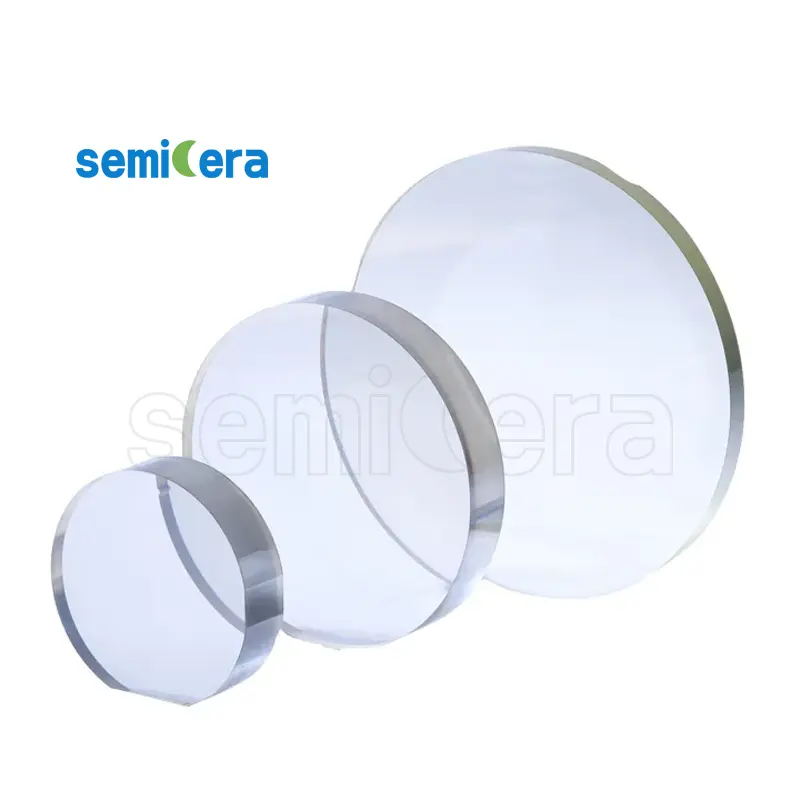
Semicera’s 4”6” High Purity Semi-Insulating SiC Ingots are designed to meet the exacting standards of the semiconductor industry. These ingots are produced with a focus on purity and consistency, making them an ideal choice for high-power and high-frequency applications where performance is paramount.
The unique properties of these SiC ingots, including high thermal conductivity and excellent electrical resistivity, make them particularly suited for use in power electronics and microwave devices. Their semi-insulating nature allows for effective heat dissipation and minimal electrical interference, leading to more efficient and reliable components.
Semicera employs state-of-the-art manufacturing processes to produce ingots with exceptional crystal quality and uniformity. This precision ensures that each ingot can be reliably used in sensitive applications, such as high-frequency amplifiers, laser diodes, and other optoelectronic devices.
Available in both 4-inch and 6-inch sizes, Semicera’s SiC ingots provide the flexibility needed for various production scales and technological requirements. Whether for research and development or mass production, these ingots deliver the performance and durability that modern electronic systems demand.
By choosing Semicera’s High Purity Semi-Insulating SiC Ingots, you are investing in a product that combines advanced material science with unparalleled manufacturing expertise. Semicera is dedicated to supporting the innovation and growth of the semiconductor industry, offering materials that enable the development of cutting-edge electronic devices.
|
アイテム |
生産 |
研究 |
ダミー |
|
クリスタルパラメーター |
|||
|
ポリタイプ |
4H |
||
|
表面向きエラー |
4±0.15° |
||
|
電気パラメーター |
|||
|
ドーパント |
N型窒素 |
||
|
抵抗率 |
0.015-0.025OHM・CM |
||
|
機械的パラメーター |
|||
|
直径 |
150.0±0.2mm |
||
|
厚さ |
350±25 µm |
||
|
一次フラットオリエンテーション |
[1-100]±5° |
||
|
プライマリフラット長 |
47.5±1.5mm |
||
|
二次フラット |
なし |
||
|
TTV |
≤5 µm |
≤10 µm |
≤15 µm |
|
LTV |
≤3μm(5mm*5mm) |
≤5μm(5mm*5mm) |
≤10μm(5mm*5mm) |
|
弓 |
-15μm〜15μm |
-35μm〜35μm |
-45μm〜45μm |
|
ワープ |
≤35 µm |
≤45 µm |
≤55 µm |
|
フロント(si-face)粗さ(AFM) |
RA≤0.2nm(5μm*5μm) |
||
|
構造 |
|||
|
マイクロパイプ密度 |
<1 EA/CM2 |
<10 EA/CM2 |
<15 EA/CM2 |
|
金属の不純物 |
≤5E10atoms/cm2 |
Na |
|
|
BPD |
≤1500 EA/CM2 |
≤3000 EA/CM2 |
Na |
|
TSD |
≤500 EA/CM2 |
≤1000 EA/CM2 |
Na |
|
フロント品質 |
|||
|
フロント |
si |
||
|
表面仕上げ |
SI-FACE CMP |
||
|
粒子 |
≤60EA/ウェーハ(サイズ以上0.3μm) |
Na |
|
|
傷 |
≤5EA/mm。累積長さ≤diameter |
累積長さ2*直径 |
Na |
|
オレンジの皮/ピット/染色/縞/亀裂/汚染 |
なし |
Na |
|
|
エッジチップ/インデント/骨折/ヘックスプレート |
なし |
||
|
ポリタイプの領域 |
なし |
累積面積≤20% |
累積面積以下30% |
|
フロントレーザーマーキング |
なし |
||
|
バック品質 |
|||
|
バックフィニッシュ |
C-Face CMP |
||
|
傷 |
≤5EA/mm、累積長さ2*直径 |
Na |
|
|
バック欠陥(エッジチップ/インデント) |
なし |
||
|
背中の粗さ |
RA≤0.2nm(5μm*5μm) |
||
|
バックレーザーマーキング |
1 mm(上端から) |
||
|
角 |
|||
|
角 |
面取り |
||
|
パッケージング |
|||
|
パッケージング |
真空パッケージングを使用したEPIの準備 マルチワーファーカセットパッケージ |
||
|
*注:「NA」とは、言及されていないリクエスト項目がSemi-STDを参照することはできないことを意味します。 |
|||


