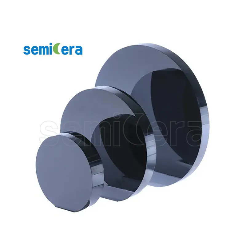
Semicera’s 4″, 6″, and 8″ N-type SiC Ingots represent a breakthrough in semiconductor materials, designed to meet the increasing demands of modern electronic and power systems. These ingots provide a robust and stable foundation for various semiconductor applications, ensuring optimal performance and longevity.
Our N-type SiC ingots are produced using advanced manufacturing processes that enhance their electrical conductivity and thermal stability. This makes them ideal for high-power and high-frequency applications, such as inverters, transistors, and other power electronic devices where efficiency and reliability are paramount.
The precise doping of these ingots ensures that they offer consistent and repeatable performance. This consistency is critical for developers and manufacturers who are pushing the boundaries of technology in fields like aerospace, automotive, and telecommunications. Semicera’s SiC ingots enable the production of devices that operate efficiently under extreme conditions.
Choosing Semicera’s N-type SiC Ingots means integrating materials that can handle high temperatures and high electrical loads with ease. These ingots are particularly suited for creating components that require excellent thermal management and high-frequency operation, such as RF amplifiers and power modules.
By opting for Semicera’s 4″, 6″, and 8″ N-type SiC Ingots, you are investing in a product that combines exceptional material properties with the precision and reliability demanded by cutting-edge semiconductor technologies. Semicera continues to lead the industry by providing innovative solutions that drive the advancement of electronic device manufacturing.
|
アイテム |
生産 |
研究 |
ダミー |
|
クリスタルパラメーター |
|||
|
ポリタイプ |
4H |
||
|
表面向きエラー |
4±0.15° |
||
|
電気パラメーター |
|||
|
ドーパント |
N型窒素 |
||
|
抵抗率 |
0.015-0.025OHM・CM |
||
|
機械的パラメーター |
|||
|
直径 |
150.0±0.2mm |
||
|
厚さ |
350±25 µm |
||
|
一次フラットオリエンテーション |
[1-100]±5° |
||
|
プライマリフラット長 |
47.5±1.5mm |
||
|
二次フラット |
なし |
||
|
TTV |
≤5 µm |
≤10 µm |
≤15 µm |
|
LTV |
≤3μm(5mm*5mm) |
≤5μm(5mm*5mm) |
≤10μm(5mm*5mm) |
|
弓 |
-15μm〜15μm |
-35μm〜35μm |
-45μm〜45μm |
|
ワープ |
≤35 µm |
≤45 µm |
≤55 µm |
|
フロント(si-face)粗さ(AFM) |
RA≤0.2nm(5μm*5μm) |
||
|
構造 |
|||
|
マイクロパイプ密度 |
<1 EA/CM2 |
<10 EA/CM2 |
<15 EA/CM2 |
|
金属の不純物 |
≤5E10atoms/cm2 |
Na |
|
|
BPD |
≤1500 EA/CM2 |
≤3000 EA/CM2 |
Na |
|
TSD |
≤500 EA/CM2 |
≤1000 EA/CM2 |
Na |
|
フロント品質 |
|||
|
フロント |
si |
||
|
表面仕上げ |
SI-FACE CMP |
||
|
粒子 |
≤60EA/ウェーハ(サイズ以上0.3μm) |
Na |
|
|
傷 |
≤5EA/mm。累積長さ≤diameter |
累積長さ2*直径 |
Na |
|
オレンジの皮/ピット/染色/縞/亀裂/汚染 |
なし |
Na |
|
|
エッジチップ/インデント/骨折/ヘックスプレート |
なし |
||
|
ポリタイプの領域 |
なし |
累積面積≤20% |
累積面積以下30% |
|
フロントレーザーマーキング |
なし |
||
|
バック品質 |
|||
|
バックフィニッシュ |
C-Face CMP |
||
|
傷 |
≤5EA/mm、累積長さ2*直径 |
Na |
|
|
バック欠陥(エッジチップ/インデント) |
なし |
||
|
背中の粗さ |
RA≤0.2nm(5μm*5μm) |
||
|
バックレーザーマーキング |
1 mm(上端から) |
||
|
角 |
|||
|
角 |
面取り |
||
|
パッケージング |
|||
|
パッケージング |
真空パッケージングを使用したEPIの準備 マルチワーファーカセットパッケージ |
||
|
*注:「NA」とは、言及されていないリクエスト項目がSemi-STDを参照することはできないことを意味します。 |
|||


