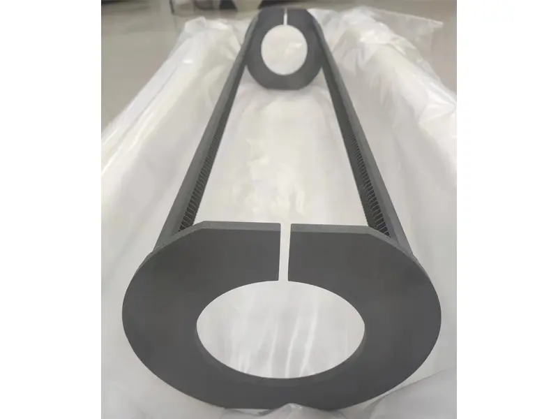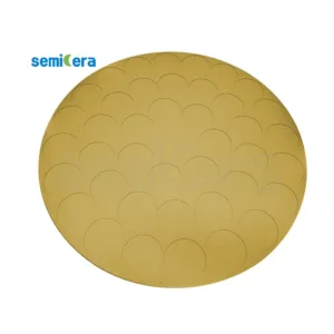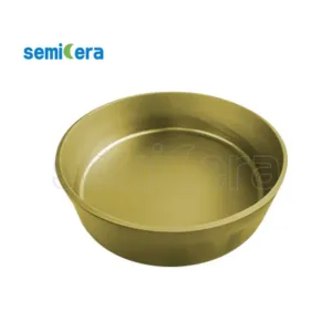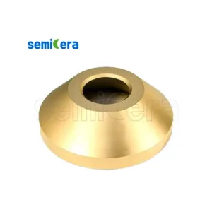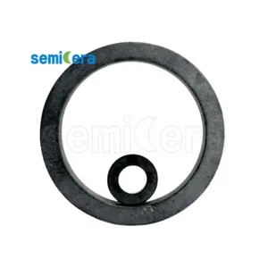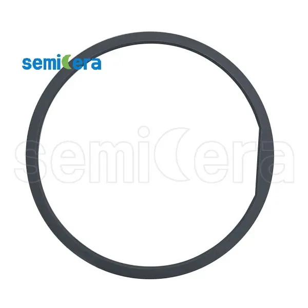
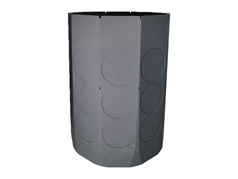
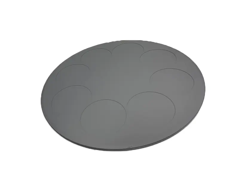
CVD Silicon Carbide(SiC) Rings offered by Semicera are key components in semiconductor etching, a vital stage in semiconductor device manufacturing. The composition of these CVD Silicon Carbide(SiC) Rings ensures a rugged and durable structure that can withstand the harsh conditions of the etching process. Chemical vapor deposition helps form a high-purity, uniform and dense SiC layer, giving the rings excellent mechanical strength, thermal stability and corrosion resistance.
As a key element in semiconductor manufacturing, CVD Silicon Carbide(SiC) Rings act as a protective barrier to protect the integrity of semiconductor chips. Its precise design ensures uniform and controlled etching, which helps in the manufacture of highly complex semiconductor devices, providing enhanced performance and reliability.
The use of CVD SiC material in the construction of the rings demonstrates a commitment to quality and performance in semiconductor manufacturing. This material has unique properties, including high thermal conductivity, excellent chemical inertness, and wear and corrosion resistance, making CVD Silicon Carbide(SiC) Rings an indispensable component in the pursuit of precision and efficiency in semiconductor etching processes.
Semicera’s CVD Silicon Carbide (SiC) Ring represents an advanced solution in the field of semiconductor manufacturing, using the unique properties of chemical vapor deposited silicon carbide to achieve reliable and high-performance etching processes, promoting the continuous advancement of semiconductor technology. We are committed to providing customers with excellent products and professional technical support to meet the semiconductor industry’s demand for high-quality and efficient etching solutions.
✓Top-quality in China market
✓Good service always for you, 7*24 hours
✓Short date of delivery
✓Small MOQ welcome and accepted
✓Custom services
エピタキシー成長受容器
シリコン/シリコンカーバイドウェーハは、電子デバイスで使用するために複数のプロセスを経る必要があります。重要なプロセスは、シリコン/sicエピタキシーで、シリコン/sicウェーハがグラファイトベースに運ばれます。 Semiceraの炭化シリコン炭化物コーティンググラファイトベースの特別な利点には、非常に高い純度、均一なコーティング、および非常に長いサービス寿命が含まれます。また、高耐性耐性と熱安定性もあります。
LEDチップ生産
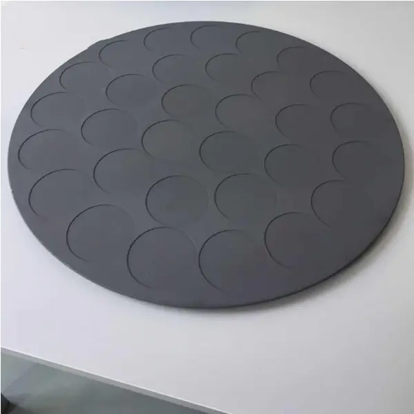
MOCVD反応器の広範なコーティング中、惑星ベースまたはキャリアが基板ウェーハを移動します。基本材料の性能は、コーティングの品質に大きな影響を与え、チップのスクラップレートに影響します。 Semiceraの炭化物コーティングベースは、高品質のLEDウェーハの製造効率を高め、波長偏差を最小限に抑えます。また、現在使用されているすべてのMOCVD反応器に追加のグラファイト成分を提供します。コンポーネントの直径が最大1.5mであっても、ほぼすべてのコンポーネントが炭化シリコンコーティングでコーティングできますが、炭化シリコンでコーティングできます。
半導体場、酸化拡散プロセス、など
半導体プロセスでは、酸化拡張プロセスには高い製品純度が必要であり、Semiceraでは、炭化シリコン部品の大部分に対してカスタムおよびCVDコーティングサービスを提供しています。
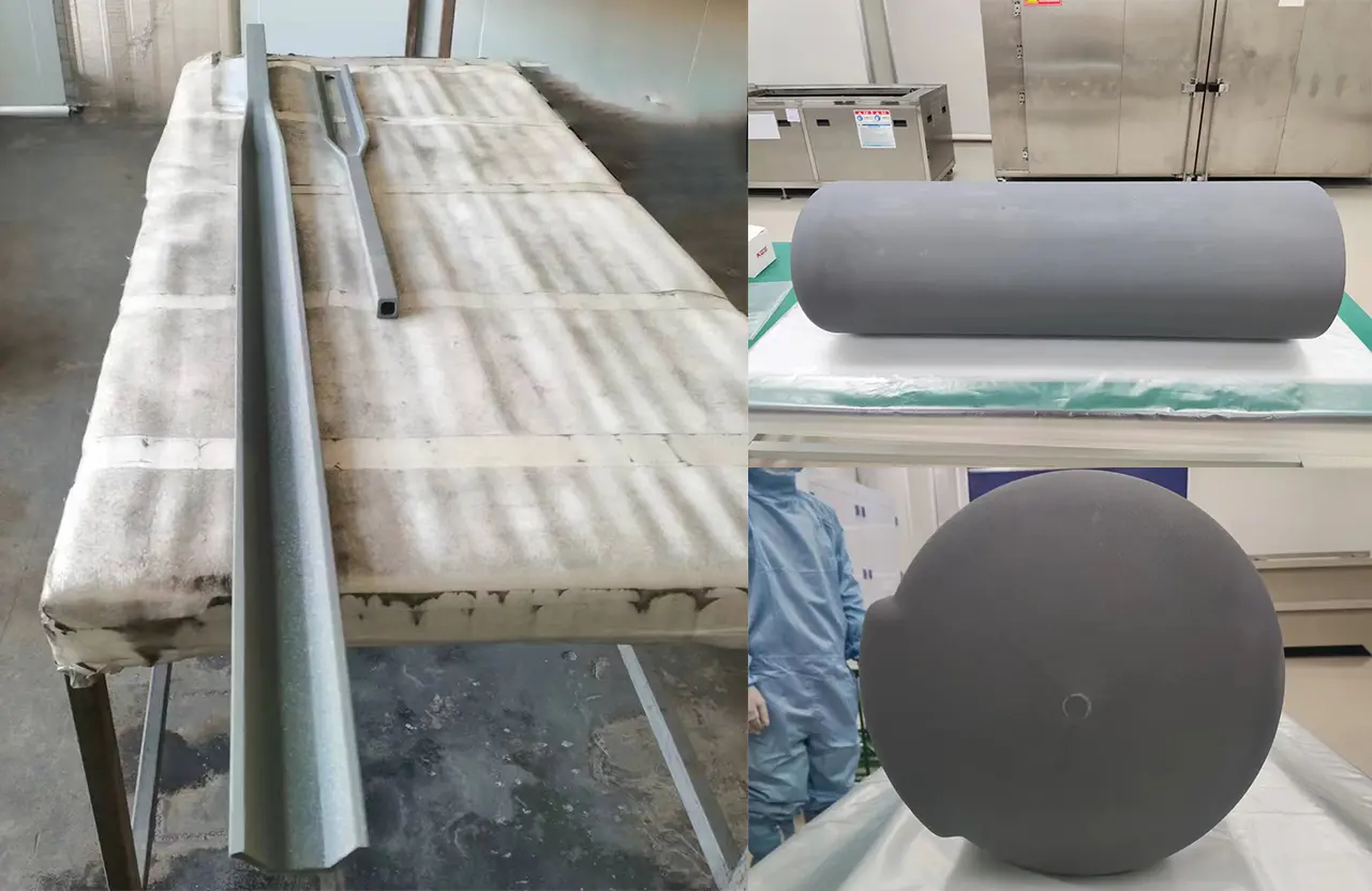
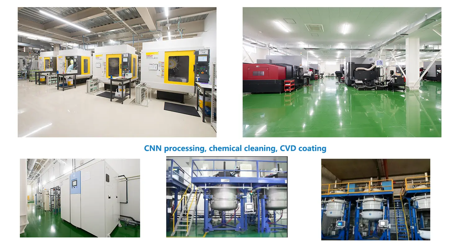
次の写真は、セミセアのラフ処理されたシリコン炭化物スラリーと100で洗浄されたシリコン炭化物炉チューブを示しています。0-レベル ダストフリー 部屋。私たちの労働者はコーティングの前に働いています。炭化シリコンの純度は99.99%に達する可能性があり、SICコーティングの純度は99.99995%を超えています.