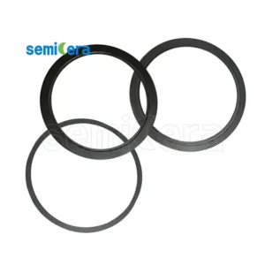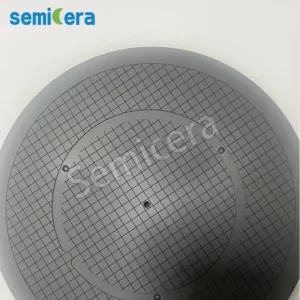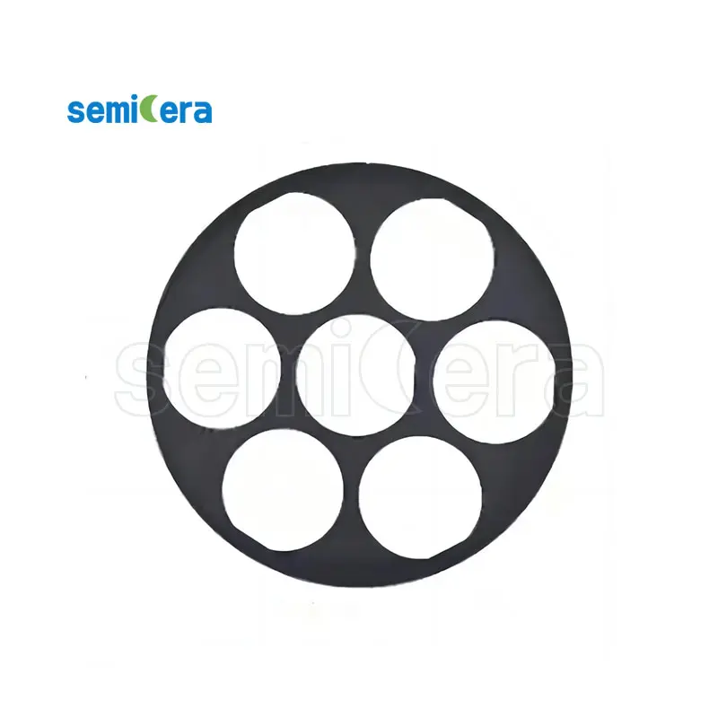
Product Description
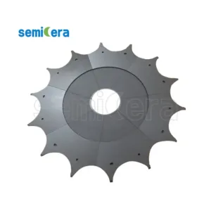
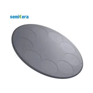
Our company provides SiC coating process services by CVD method on the surface of graphite, ceramics and other materials, so that special gases containing carbon and silicon react at high temperature to obtain high purity SiC molecules, molecules deposited on the surface of the coated materials, forming SIC protective layer.
主な機能:
1。高温酸化抵抗:
温度が1600 Cになると、酸化抵抗は非常に良好です。
2. High purity : made by chemical vapor deposition under high temperature chlorination condition.
3。侵食抵抗:高硬度、コンパクトな表面、微粒子。
4。耐食性:酸、アルカリ、塩、有機試薬。


CVD-SICコーティングの主な仕様
|
SIC-CVDプロパティ |
||
|
結晶構造 |
FCCβ相 |
|
|
密度 |
g/cm³ |
3.21 |
|
硬度 |
ビッカーズの硬さ |
2500 |
|
穀物サイズ |
mm |
2~10 |
|
化学純度 |
% |
99.99995 |
|
熱容量 |
J・kg-1・k-1 |
640 |
|
昇華温度 |
℃ |
2700 |
|
フェレキュラルの強さ |
MPA(RT 4ポイント) |
415 |
|
ヤングモジュラス |
GPA(4ptベンド、1300℃) |
430 |
|
熱膨張(CTE) |
10-6K-1 |
4.5 |
|
熱伝導率 |
(w/mk) |
300 |