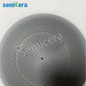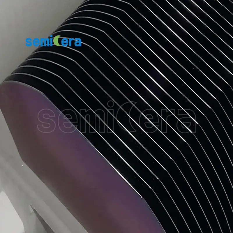
Silicon on Insulator Wafers from Semicera are designed to meet the growing demand for high-performance semiconductor solutions. Our SOI wafers offer superior electrical performance and reduced parasitic device capacitance, making them ideal for advanced applications such as MEMS devices, sensors, and integrated circuits. Semicera’s expertise in wafer production ensures that each SOI wafer provides reliable, high-quality results for your next-generation technology needs.
Our Silicon on Insulator Wafers offer an optimal balance between cost-effectiveness and performance. With soi wafer cost becoming increasingly competitive, these wafers are widely used in a range of industries, including microelectronics and optoelectronics. Semicera’s high-precision production process guarantees superior wafer bonding and uniformity, making them suitable for a variety of applications, from cavity SOI wafers to standard silicon wafers.
重要な機能:
• High-quality SOI wafers optimized for performance in MEMS and other applications.
• Competitive soi wafer cost for businesses seeking advanced solutions without compromising quality.
• Ideal for cutting-edge technologies, offering enhanced electrical isolation and efficiency in silicon on insulator systems.
Our Silicon on Insulator Wafers are engineered to provide high-performance solutions, supporting the next wave of innovation in semiconductor technology. Whether you’re working on cavity SOI wafers, MEMS devices, or silicon on insulator components, Semicera delivers wafers that meet the highest standards in the industry.
|
アイテム |
生産 |
研究 |
ダミー |
|
クリスタルパラメーター |
|||
|
ポリタイプ |
4H |
||
|
表面向きエラー |
<11-20 >4±0.15° |
||
|
電気パラメーター |
|||
|
ドーパント |
N型窒素 |
||
|
抵抗率 |
0.015-0.025ohm·cm |
||
|
機械的パラメーター |
|||
|
直径 |
150.0±0.2mm |
||
|
厚さ |
350±25 μm |
||
|
一次フラットオリエンテーション |
[1-100]±5° |
||
|
プライマリフラット長 |
47.5±1.5mm |
||
|
二次フラット |
なし |
||
|
TTV |
≤5 μm |
≤10 μm |
≤15 μm |
|
LTV |
≤3 μm(5mm*5mm) |
≤5 μm(5mm*5mm) |
≤10 μm(5mm*5mm) |
|
弓 |
-15μm ~ 15μm |
-35μm ~ 35μm |
-45μm ~ 45μm |
|
ワープ |
≤35 μm |
≤45 μm |
≤55 μm |
|
フロント(si-face)粗さ(AFM) |
Ra≤0.2nm (5μm*5μm) |
||
|
構造 |
|||
|
マイクロパイプ密度 |
<1 EA/CM2 |
<10 EA/CM2 |
<15 EA/CM2 |
|
金属の不純物 |
≤5E10atoms/cm2 |
Na |
|
|
BPD |
≤1500 ea/cm2 |
≤3000 ea/cm2 |
Na |
|
TSD |
≤500 ea/cm2 |
≤1000 ea/cm2 |
Na |
|
フロント品質 |
|||
|
フロント |
si |
||
|
表面仕上げ |
SI-FACE CMP |
||
|
粒子 |
≤60ea/wafer (size≥0.3μm) |
Na |
|
|
傷 |
≤5ea/mm. Cumulative length ≤Diameter |
Cumulative length≤2*Diameter |
Na |
|
オレンジの皮/ピット/染色/縞/亀裂/汚染 |
なし |
Na |
|
|
エッジチップ/インデント/骨折/ヘックスプレート |
なし |
||
|
ポリタイプの領域 |
なし |
Cumulative area≤20% |
Cumulative area≤30% |
|
フロントレーザーマーキング |
なし |
||
|
バック品質 |
|||
|
バックフィニッシュ |
C-Face CMP |
||
|
傷 |
≤5ea/mm,Cumulative length≤2*Diameter |
Na |
|
|
バック欠陥(エッジチップ/インデント) |
なし |
||
|
背中の粗さ |
Ra≤0.2nm (5μm*5μm) |
||
|
バックレーザーマーキング |
1 mm(上端から) |
||
|
角 |
|||
|
角 |
面取り |
||
|
パッケージング |
|||
|
パッケージング |
真空パッケージングを使用したEPIの準備 マルチワーファーカセットパッケージ |
||
|
*Notes: “NA” means no request Items not mentioned may refer to SEMI-STD. |
|||