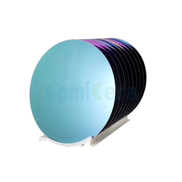
The SOI wafer is a sandwich-like structure with three layers; Including the top layer (device layer), the middle of the buried oxygen layer (for the insulating SiO2 layer) and the bottom substrate (bulk silicon). SOI wafers are produced using the SIMOX method and wafer bonding technology, which allows for thinner and more accurate device layers, uniform thickness and low defect density.

Application field
1. High-speed integrated circuit
2. Microwave devices
3. High temperature integrated circuit
4. Power devices
5. Low power integrated circuit
6. MEMS
7. Low voltage integrated circuit
|
Item |
Argument |
|
|
Overall |
Wafer Diameter |
50/75/100/125/150/200mm±25um |
|
Bow/Warp |
<10um |
|
|
粒子 |
0.3um<30ea |
|
|
Flats/Notch |
Flat or Notch |
|
|
Edge Exclusion |
/ |
|
|
Device Layer |
Device-layer Type/Dopant |
N-Type/P-Type |
|
Device-layer Orientation |
<1-0-0> / <1-1-1> / <1-1-0> |
|
|
Device-layer Thickness |
0.1~300um |
|
|
Device-layer Resistivity |
0.001~100,000 ohm-cm |
|
|
Device-layer Particles |
<30ea@0.3 |
|
|
Device Layer TTV |
<10um |
|
|
Device Layer Finish |
Polished |
|
|
BOX |
Buried Thermal Oxide Thickness |
50nm(500Å)~15um |
|
Handle Layer |
Handle Wafer Type/Dopant |
N-Type/P-Type |
|
Handle Wafer Orientation |
<1-0-0> / <1-1-1> / <1-1-0> |
|
|
Handle Wafer Resistivity |
0.001~100,000 ohm-cm |
|
|
Handle Wafer Thickness |
>100um |
|
|
Handle Wafer Finish |
Polished |
|
|
SOI wafers of target specifications can be customized according to customer requirements. |
||
