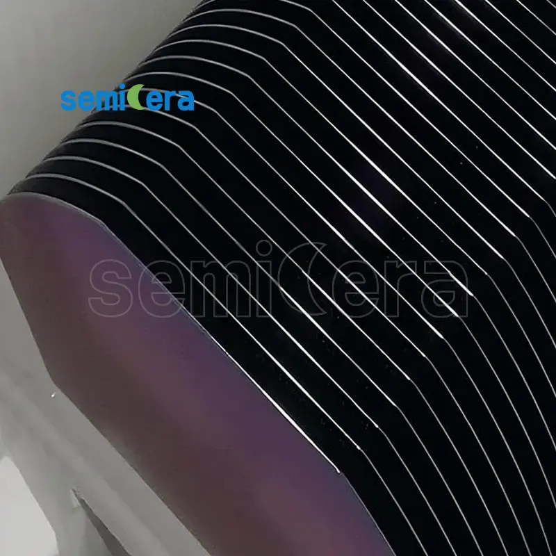
Silicon on Insulator Wafers from Semicera are designed to meet the growing demand for high-performance semiconductor solutions. Our SOI wafers offer superior electrical performance and reduced parasitic device capacitance, making them ideal for advanced applications such as MEMS devices, sensors, and integrated circuits. Semicera’s expertise in wafer production ensures that each SOI wafer provides reliable, high-quality results for your next-generation technology needs.
Our Silicon on Insulator Wafers offer an optimal balance between cost-effectiveness and performance. With soi wafer cost becoming increasingly competitive, these wafers are widely used in a range of industries, including microelectronics and optoelectronics. Semicera’s high-precision production process guarantees superior wafer bonding and uniformity, making them suitable for a variety of applications, from cavity SOI wafers to standard silicon wafers.
주요 기능:
• High-quality SOI wafers optimized for performance in MEMS and other applications.
• Competitive soi wafer cost for businesses seeking advanced solutions without compromising quality.
• Ideal for cutting-edge technologies, offering enhanced electrical isolation and efficiency in silicon on insulator systems.
Our Silicon on Insulator Wafers are engineered to provide high-performance solutions, supporting the next wave of innovation in semiconductor technology. Whether you’re working on cavity SOI wafers, MEMS devices, or silicon on insulator components, Semicera delivers wafers that meet the highest standards in the industry.
|
항목 |
생산 |
연구 |
더미 |
|
결정 매개 변수 |
|||
|
폴리 타입 |
4H |
||
|
표면 방향 오류 |
<11-20 >4±0.15° |
||
|
전기 매개 변수 |
|||
|
도펀트 |
N- 타입 질소 |
||
|
저항 |
0.015-0.025ohm·cm |
||
|
기계적 매개 변수 |
|||
|
지름 |
150.0±0.2mm |
||
|
두께 |
350±25 μm |
||
|
1 차 평평한 방향 |
[1-100]±5° |
||
|
1 차 평평한 길이 |
47.5±1.5mm |
||
|
보조 아파트 |
없음 |
||
|
TTV |
≤5 μm |
≤10 μm |
≤15 μm |
|
LTV |
≤3 μm(5mm*5mm) |
≤5 μm(5mm*5mm) |
≤10 μm(5mm*5mm) |
|
절하다 |
-15μm ~ 15μm |
-35μm ~ 35μm |
-45μm ~ 45μm |
|
경사 |
≤35 μm |
≤45 μm |
≤55 μm |
|
전면 (si-face) 거칠기 (AFM) |
Ra≤0.2nm (5μm*5μm) |
||
|
구조 |
|||
|
마이크로 파이프 밀도 |
<1 EA/CM2 |
<10 EA/CM2 |
<15 EA/CM2 |
|
금속 불순물 |
≤5E10atoms/cm2 |
NA |
|
|
BPD |
≤1500 ea/cm2 |
≤3000 ea/cm2 |
NA |
|
TSD |
≤500 ea/cm2 |
≤1000 ea/cm2 |
NA |
|
프론트 품질 |
|||
|
앞쪽 |
시 |
||
|
표면 마감 |
Si-Face CMP |
||
|
입자 |
≤60ea/wafer (size≥0.3μm) |
NA |
|
|
흠집 |
≤5ea/mm. Cumulative length ≤Diameter |
Cumulative length≤2*Diameter |
NA |
|
오렌지 껍질/구덩이/얼룩/줄무늬/균열/오염 |
없음 |
NA |
|
|
에지 칩/인테이션/골절/육각 플레이트 |
없음 |
||
|
폴리 타입 영역 |
없음 |
Cumulative area≤20% |
Cumulative area≤30% |
|
전면 레이저 표시 |
없음 |
||
|
뒤로 품질 |
|||
|
뒤로 마무리 |
C-Face CMP |
||
|
흠집 |
≤5ea/mm,Cumulative length≤2*Diameter |
NA |
|
|
등 결함 (Edge Chips/Indents) |
없음 |
||
|
뒤로 거칠기 |
Ra≤0.2nm (5μm*5μm) |
||
|
뒤 레이저 표시 |
1 mm (상단 가장자리에서) |
||
|
가장자리 |
|||
|
가장자리 |
모따기 |
||
|
포장 |
|||
|
포장 |
진공 포장으로 에피 레디 멀티 웨이 커 카세트 포장 |
||
|
*Notes: “NA” means no request Items not mentioned may refer to SEMI-STD. |
|||