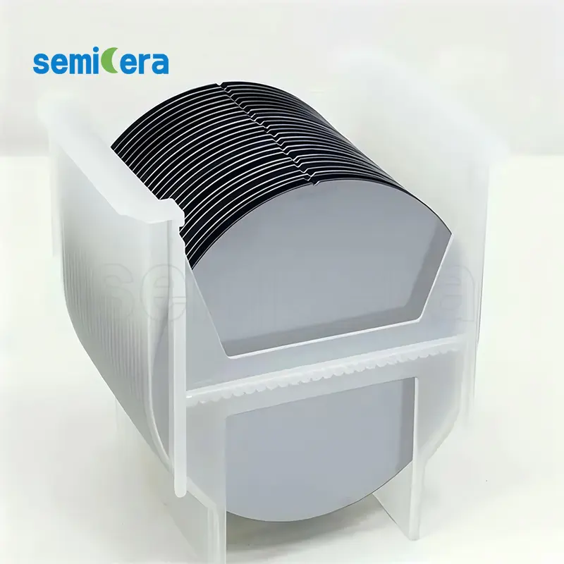
Semicera introduces the Wafer Cassette Carrier, a critical solution for the secure and efficient handling of semiconductor wafers. This carrier is engineered to meet the stringent requirements of the semiconductor industry, ensuring the protection and integrity of your wafers throughout the manufacturing process.
주요 기능:
• Robust Construction: 그만큼 Wafer Cassette Carrier is built from high-quality, durable materials that withstand the rigors of semiconductor environments, providing reliable protection against contamination and physical damage.
• Precise Alignment: Designed for precise wafer alignment, this carrier ensures that wafers are securely held in place, minimizing the risk of misalignment or damage during transport.
• Easy Handling: Ergonomically designed for ease of use, the carrier simplifies the loading and unloading process, improving workflow efficiency in cleanroom environments.
• Compatibility: Compatible with a wide range of wafer sizes and types, making it versatile for various semiconductor manufacturing needs.
Experience unparalleled protection and convenience with Semicera’s Wafer Cassette Carrier. Our carrier is designed to meet the highest standards of semiconductor manufacturing, ensuring your wafers remain in pristine condition from start to finish. Trust Semicera to deliver the quality and reliability you need for your most critical processes.
|
항목 |
생산 |
연구 |
더미 |
|
결정 매개 변수 |
|||
|
폴리 타입 |
4H |
||
|
표면 방향 오류 |
4±0.15° |
||
|
전기 매개 변수 |
|||
|
도펀트 |
N- 타입 질소 |
||
|
저항 |
0.015-0.025ohm · cm |
||
|
기계적 매개 변수 |
|||
|
지름 |
150.0 ± 0.2mm |
||
|
두께 |
350 ± 25 µm |
||
|
1 차 평평한 방향 |
[1-100]±5° |
||
|
1 차 평평한 길이 |
47.5 ± 1.5mm |
||
|
보조 아파트 |
없음 |
||
|
TTV |
≤5 µm |
≤10 µm |
≤15 µm |
|
LTV |
≤3 μm (5mm*5mm) |
≤5 μm (5mm*5mm) |
≤10 μm (5mm*5mm) |
|
절하다 |
-15μm ~ 15μm |
-35μm ~ 35μm |
-45μm ~ 45μm |
|
경사 |
≤35 µm |
≤45 µm |
≤55 µm |
|
전면 (si-face) 거칠기 (AFM) |
Ra≤0.2nm (5μm*5μm) |
||
|
구조 |
|||
|
마이크로 파이프 밀도 |
<1 EA/CM2 |
<10 EA/CM2 |
<15 EA/CM2 |
|
금속 불순물 |
≤5E10atoms/cm2 |
NA |
|
|
BPD |
≤1500 EA/CM2 |
≤3000 EA/CM2 |
NA |
|
TSD |
≤500 EA/CM2 |
≤1000 EA/CM2 |
NA |
|
프론트 품질 |
|||
|
앞쪽 |
시 |
||
|
표면 마감 |
Si-Face CMP |
||
|
입자 |
≤60EA/웨이퍼 (크기 0.3μm) |
NA |
|
|
흠집 |
≤5EA/mm. 누적 길이 ≤ diameter |
누적 길이 ≤2*직경 |
NA |
|
오렌지 껍질/구덩이/얼룩/줄무늬/균열/오염 |
없음 |
NA |
|
|
에지 칩/인테이션/골절/육각 플레이트 |
없음 |
||
|
폴리 타입 영역 |
없음 |
누적 면적 ≤20% |
누적 면적 ≤30% |
|
전면 레이저 표시 |
없음 |
||
|
뒤로 품질 |
|||
|
뒤로 마무리 |
C-Face CMP |
||
|
흠집 |
≤5EA/mm, 누적 길이 ≤2*직경 |
NA |
|
|
등 결함 (Edge Chips/Indents) |
없음 |
||
|
뒤로 거칠기 |
Ra≤0.2nm (5μm*5μm) |
||
|
뒤 레이저 표시 |
1 mm (상단 가장자리에서) |
||
|
가장자리 |
|||
|
가장자리 |
모따기 |
||
|
포장 |
|||
|
포장 |
진공 포장으로 에피 레디 멀티 웨이 커 카세트 포장 |
||
|
*참고 :“NA”는 언급되지 않은 요청 항목이 Semi-STD를 참조 할 수 없음을 의미합니다. |
|||


