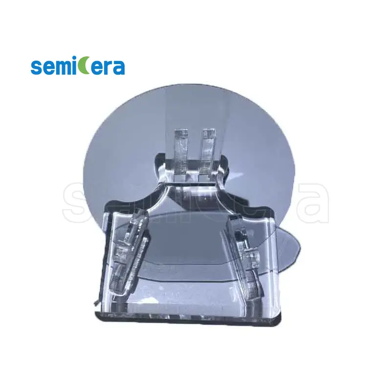
세미카 is excited to offer 2″ Gallium Oxide Substrates, a cutting-edge material designed to enhance the performance of advanced semiconductor devices. These substrates, made from Gallium Oxide (Ga2O3), feature an ultra-wide bandgap, making them an ideal choice for high-power, high-frequency, and UV optoelectronic applications.
주요 기능:
• Ultra-Wide Bandgap: 그만큼 2″ Gallium Oxide Substrates provide an outstanding bandgap of approximately 4.8 eV, allowing for higher voltage and temperature operation, far exceeding the capabilities of traditional semiconductor materials like silicon.
• Exceptional Breakdown Voltage: These substrates enable devices to handle significantly higher voltages, making them perfect for power electronics, especially in high-voltage applications.
• Excellent Thermal Conductivity: With superior thermal stability, these substrates maintain consistent performance even in extreme thermal environments, ideal for high-power and high-temperature applications.
• High-Quality Material: 그만큼 2″ Gallium Oxide Substrates offer low defect densities and high crystalline quality, ensuring the reliable and efficient performance of your semiconductor devices.
• 다목적 응용 프로그램: These substrates are suited for a range of applications, including power transistors, Schottky diodes, and UV-C LED devices, offering a robust foundation for both power and optoelectronic innovations.
Unlock the full potential of your semiconductor devices with Semicera’s 2″ Gallium Oxide Substrates. Our substrates are designed to meet the demanding needs of today’s advanced applications, ensuring high performance, reliability, and efficiency. Choose Semicera for state-of-the-art semiconductor materials that drive innovation.
|
항목 |
생산 |
연구 |
더미 |
|
결정 매개 변수 |
|||
|
폴리 타입 |
4H |
||
|
표면 방향 오류 |
4±0.15° |
||
|
전기 매개 변수 |
|||
|
도펀트 |
N- 타입 질소 |
||
|
저항 |
0.015-0.025ohm · cm |
||
|
기계적 매개 변수 |
|||
|
지름 |
150.0 ± 0.2mm |
||
|
두께 |
350 ± 25 µm |
||
|
1 차 평평한 방향 |
[1-100]±5° |
||
|
1 차 평평한 길이 |
47.5 ± 1.5mm |
||
|
보조 아파트 |
없음 |
||
|
TTV |
≤5 µm |
≤10 µm |
≤15 µm |
|
LTV |
≤3 μm (5mm*5mm) |
≤5 μm (5mm*5mm) |
≤10 μm (5mm*5mm) |
|
절하다 |
-15μm ~ 15μm |
-35μm ~ 35μm |
-45μm ~ 45μm |
|
경사 |
≤35 µm |
≤45 µm |
≤55 µm |
|
전면 (si-face) 거칠기 (AFM) |
Ra≤0.2nm (5μm*5μm) |
||
|
구조 |
|||
|
마이크로 파이프 밀도 |
<1 EA/CM2 |
<10 EA/CM2 |
<15 EA/CM2 |
|
금속 불순물 |
≤5E10atoms/cm2 |
NA |
|
|
BPD |
≤1500 EA/CM2 |
≤3000 EA/CM2 |
NA |
|
TSD |
≤500 EA/CM2 |
≤1000 EA/CM2 |
NA |
|
프론트 품질 |
|||
|
앞쪽 |
시 |
||
|
표면 마감 |
Si-Face CMP |
||
|
입자 |
≤60EA/웨이퍼 (크기 0.3μm) |
NA |
|
|
흠집 |
≤5EA/mm. 누적 길이 ≤ diameter |
누적 길이 ≤2*직경 |
NA |
|
오렌지 껍질/구덩이/얼룩/줄무늬/균열/오염 |
없음 |
NA |
|
|
에지 칩/인테이션/골절/육각 플레이트 |
없음 |
||
|
폴리 타입 영역 |
없음 |
누적 면적 ≤20% |
누적 면적 ≤30% |
|
전면 레이저 표시 |
없음 |
||
|
뒤로 품질 |
|||
|
뒤로 마무리 |
C-Face CMP |
||
|
흠집 |
≤5EA/mm, 누적 길이 ≤2*직경 |
NA |
|
|
등 결함 (Edge Chips/Indents) |
없음 |
||
|
뒤로 거칠기 |
Ra≤0.2nm (5μm*5μm) |
||
|
뒤 레이저 표시 |
1 mm (상단 가장자리에서) |
||
|
가장자리 |
|||
|
가장자리 |
모따기 |
||
|
포장 |
|||
|
포장 |
진공 포장으로 에피 레디 멀티 웨이 커 카세트 포장 |
||
|
*참고 :“NA”는 언급되지 않은 요청 항목이 Semi-STD를 참조 할 수 없음을 의미합니다. |
|||