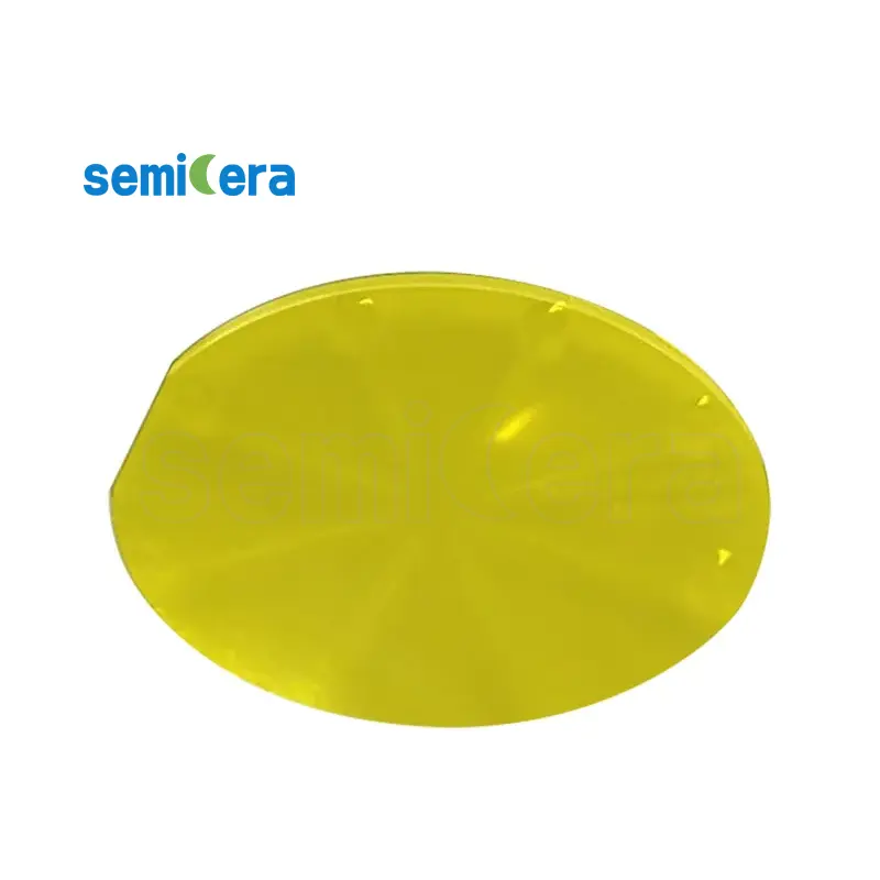
Semicera 3C-SiC Wafer Substrates are engineered to provide a robust platform for next-generation power electronics and high-frequency devices. With superior thermal properties and electrical characteristics, these substrates are designed to meet the demanding requirements of modern technology.
The 3C-SiC (Cubic Silicon Carbide) structure of Semicera Wafer Substrates offers unique advantages, including higher thermal conductivity and a lower thermal expansion coefficient compared to other semiconductor materials. This makes them an excellent choice for devices operating under extreme temperatures and high-power conditions.
With a high electrical breakdown voltage and superior chemical stability, Semicera 3C-SiC Wafer Substrates ensure long-lasting performance and reliability. These properties are critical for applications such as high-frequency radar, solid-state lighting, and power inverters, where efficiency and durability are paramount.
Semicera’s commitment to quality is reflected in the meticulous manufacturing process of their 3C-SiC Wafer Substrates, ensuring uniformity and consistency across every batch. This precision contributes to the overall performance and longevity of the electronic devices built upon them.
By choosing Semicera 3C-SiC Wafer Substrates, manufacturers gain access to a cutting-edge material that enables the development of smaller, faster, and more efficient electronic components. Semicera continues to support technological innovation by providing reliable solutions that meet the evolving demands of the semiconductor industry.
|
항목 |
생산 |
연구 |
더미 |
|
결정 매개 변수 |
|||
|
폴리 타입 |
4H |
||
|
표면 방향 오류 |
4±0.15° |
||
|
전기 매개 변수 |
|||
|
도펀트 |
N- 타입 질소 |
||
|
저항 |
0.015-0.025ohm · cm |
||
|
기계적 매개 변수 |
|||
|
지름 |
150.0 ± 0.2mm |
||
|
두께 |
350 ± 25 µm |
||
|
1 차 평평한 방향 |
[1-100]±5° |
||
|
1 차 평평한 길이 |
47.5 ± 1.5mm |
||
|
보조 아파트 |
없음 |
||
|
TTV |
≤5 µm |
≤10 µm |
≤15 µm |
|
LTV |
≤3 μm (5mm*5mm) |
≤5 μm (5mm*5mm) |
≤10 μm (5mm*5mm) |
|
절하다 |
-15μm ~ 15μm |
-35μm ~ 35μm |
-45μm ~ 45μm |
|
경사 |
≤35 µm |
≤45 µm |
≤55 µm |
|
전면 (si-face) 거칠기 (AFM) |
Ra≤0.2nm (5μm*5μm) |
||
|
구조 |
|||
|
마이크로 파이프 밀도 |
<1 EA/CM2 |
<10 EA/CM2 |
<15 EA/CM2 |
|
금속 불순물 |
≤5E10atoms/cm2 |
NA |
|
|
BPD |
≤1500 EA/CM2 |
≤3000 EA/CM2 |
NA |
|
TSD |
≤500 EA/CM2 |
≤1000 EA/CM2 |
NA |
|
프론트 품질 |
|||
|
앞쪽 |
시 |
||
|
표면 마감 |
Si-Face CMP |
||
|
입자 |
≤60EA/웨이퍼 (크기 0.3μm) |
NA |
|
|
흠집 |
≤5EA/mm. 누적 길이 ≤ diameter |
누적 길이 ≤2*직경 |
NA |
|
오렌지 껍질/구덩이/얼룩/줄무늬/균열/오염 |
없음 |
NA |
|
|
에지 칩/인테이션/골절/육각 플레이트 |
없음 |
||
|
폴리 타입 영역 |
없음 |
누적 면적 ≤20% |
누적 면적 ≤30% |
|
전면 레이저 표시 |
없음 |
||
|
뒤로 품질 |
|||
|
뒤로 마무리 |
C-Face CMP |
||
|
흠집 |
≤5EA/mm, 누적 길이 ≤2*직경 |
NA |
|
|
등 결함 (Edge Chips/Indents) |
없음 |
||
|
뒤로 거칠기 |
Ra≤0.2nm (5μm*5μm) |
||
|
뒤 레이저 표시 |
1 mm (상단 가장자리에서) |
||
|
가장자리 |
|||
|
가장자리 |
모따기 |
||
|
포장 |
|||
|
포장 |
진공 포장으로 에피 레디 멀티 웨이 커 카세트 포장 |
||
|
*참고 :“NA”는 언급되지 않은 요청 항목이 Semi-STD를 참조 할 수 없음을 의미합니다. |
|||


