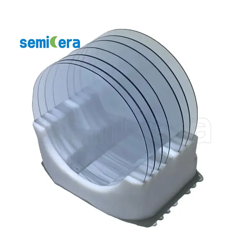
세미카 proudly introduces its 4″ Gallium Oxide Substrates, a groundbreaking material engineered to meet the growing demands of high-performance semiconductor devices. Gallium Oxide (Ga2O3) substrates offer an ultra-wide bandgap, making them ideal for next-generation power electronics, UV optoelectronics, and high-frequency devices.
주요 기능:
• Ultra-Wide Bandgap: 그만큼 4″ Gallium Oxide Substrates boast a bandgap of approximately 4.8 eV, allowing for exceptional voltage and temperature tolerance, significantly outperforming traditional semiconductor materials like silicon.
• High Breakdown Voltage: These substrates enable devices to operate at higher voltages and powers, making them perfect for high-voltage applications in power electronics.
• Superior Thermal Stability: Gallium Oxide substrates offer excellent thermal conductivity, ensuring stable performance under extreme conditions, ideal for use in demanding environments.
• High Material Quality: With low defect densities and high crystal quality, these substrates ensure reliable and consistent performance, enhancing the efficiency and durability of your devices.
• Versatile Application: Suitable for a wide range of applications, including power transistors, Schottky diodes, and UV-C LED devices, enabling innovations in both power and optoelectronic fields.
Explore the future of semiconductor technology with Semicera’s 4″ Gallium Oxide Substrates. Our substrates are designed to support the most advanced applications, providing the reliability and efficiency required for today’s cutting-edge devices. Trust Semicera for quality and innovation in your semiconductor materials.
|
항목 |
생산 |
연구 |
더미 |
|
결정 매개 변수 |
|||
|
폴리 타입 |
4H |
||
|
표면 방향 오류 |
4±0.15° |
||
|
전기 매개 변수 |
|||
|
도펀트 |
N- 타입 질소 |
||
|
저항 |
0.015-0.025ohm · cm |
||
|
기계적 매개 변수 |
|||
|
지름 |
150.0 ± 0.2mm |
||
|
두께 |
350 ± 25 µm |
||
|
1 차 평평한 방향 |
[1-100]±5° |
||
|
1 차 평평한 길이 |
47.5 ± 1.5mm |
||
|
보조 아파트 |
없음 |
||
|
TTV |
≤5 µm |
≤10 µm |
≤15 µm |
|
LTV |
≤3 μm (5mm*5mm) |
≤5 μm (5mm*5mm) |
≤10 μm (5mm*5mm) |
|
절하다 |
-15μm ~ 15μm |
-35μm ~ 35μm |
-45μm ~ 45μm |
|
경사 |
≤35 µm |
≤45 µm |
≤55 µm |
|
전면 (si-face) 거칠기 (AFM) |
Ra≤0.2nm (5μm*5μm) |
||
|
구조 |
|||
|
마이크로 파이프 밀도 |
<1 EA/CM2 |
<10 EA/CM2 |
<15 EA/CM2 |
|
금속 불순물 |
≤5E10atoms/cm2 |
NA |
|
|
BPD |
≤1500 EA/CM2 |
≤3000 EA/CM2 |
NA |
|
TSD |
≤500 EA/CM2 |
≤1000 EA/CM2 |
NA |
|
프론트 품질 |
|||
|
앞쪽 |
시 |
||
|
표면 마감 |
Si-Face CMP |
||
|
입자 |
≤60EA/웨이퍼 (크기 0.3μm) |
NA |
|
|
흠집 |
≤5EA/mm. 누적 길이 ≤ diameter |
누적 길이 ≤2*직경 |
NA |
|
오렌지 껍질/구덩이/얼룩/줄무늬/균열/오염 |
없음 |
NA |
|
|
에지 칩/인테이션/골절/육각 플레이트 |
없음 |
||
|
폴리 타입 영역 |
없음 |
누적 면적 ≤20% |
누적 면적 ≤30% |
|
전면 레이저 표시 |
없음 |
||
|
뒤로 품질 |
|||
|
뒤로 마무리 |
C-Face CMP |
||
|
흠집 |
≤5EA/mm, 누적 길이 ≤2*직경 |
NA |
|
|
등 결함 (Edge Chips/Indents) |
없음 |
||
|
뒤로 거칠기 |
Ra≤0.2nm (5μm*5μm) |
||
|
뒤 레이저 표시 |
1 mm (상단 가장자리에서) |
||
|
가장자리 |
|||
|
가장자리 |
모따기 |
||
|
포장 |
|||
|
포장 |
진공 포장으로 에피 레디 멀티 웨이 커 카세트 포장 |
||
|
*참고 :“NA”는 언급되지 않은 요청 항목이 Semi-STD를 참조 할 수 없음을 의미합니다. |
|||


