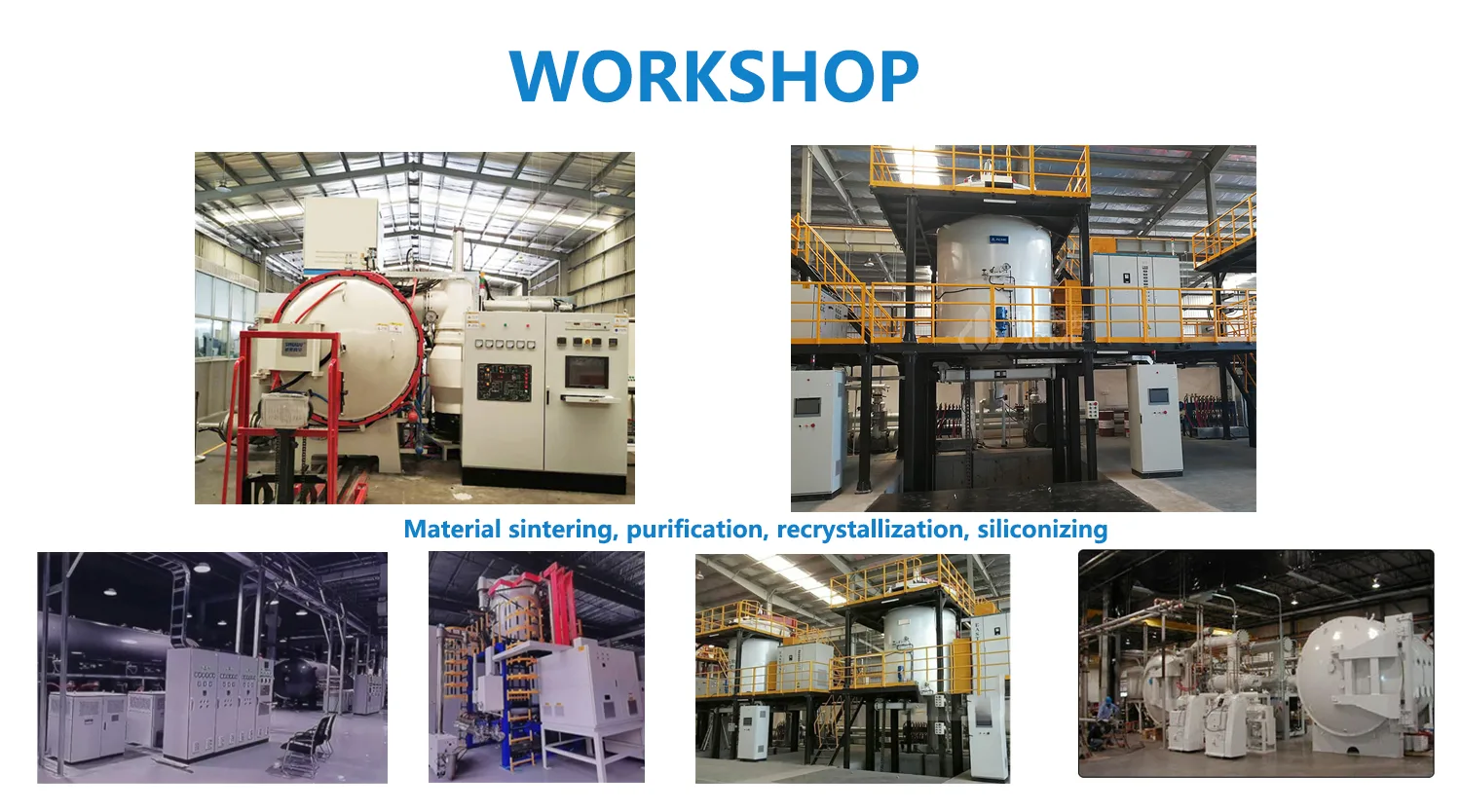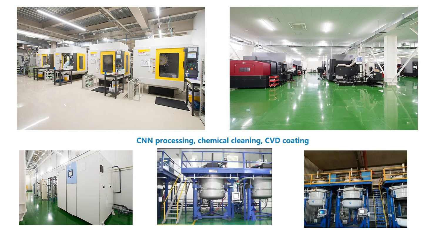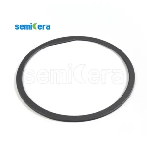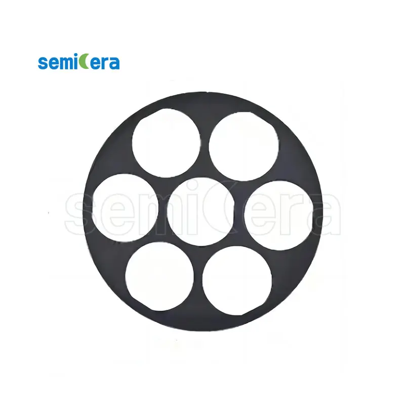
Product Description
Our company provides SiC coating process services by CVD method on the surface of graphite, ceramics and other materials, so that special gases containing carbon and silicon react at high temperature to obtain high purity SiC molecules, molecules deposited on the surface of the coated materials, forming SIC protective layer.
주요 기능:
1. 고온 산화 저항:
온도가 1600 C에 이르면 산화 저항은 여전히 매우 좋습니다.
2. High purity : made by chemical vapor deposition under high temperature chlorination condition.
3. 침식 저항 : 높은 경도, 소형 표면, 미세 입자.
4. 부식성 : 산, 알칼리, 소금 및 유기 시약.


CVD-SIC 코팅의 주요 사양
|
SIC-CVD 특성 |
||
|
결정 구조 |
FCC β 상 |
|
|
밀도 |
g/cm ³ |
3.21 |
|
경도 |
비커스 경도 |
2500 |
|
곡물 크기 |
mm |
2~10 |
|
화학적 순도 |
% |
99.99995 |
|
열용량 |
J · KG-1 · K-1 |
640 |
|
승화 온도 |
℃ |
2700 |
|
Felexural 강도 |
MPA (RT 4 점) |
415 |
|
Young’ s Modulus |
GPA (4pt Bend, 1300 ℃) |
430 |
|
열 팽창 (CTE) |
10-6K-1 |
4.5 |
|
열전도율 |
(w/mk) |
300 |