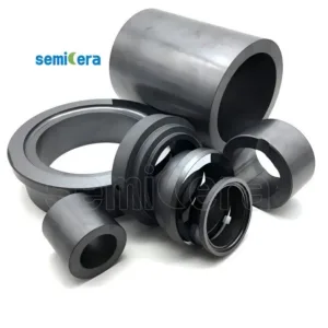
Silicon on Insulator Wafers from Semicera are designed to meet the growing demand for high-performance semiconductor solutions. Our SOI wafers offer superior electrical performance and reduced parasitic device capacitance, making them ideal for advanced applications such as MEMS devices, sensors, and integrated circuits. Semicera’s expertise in wafer production ensures that each SOI wafer provides reliable, high-quality results for your next-generation technology needs.
Our Silicon on Insulator Wafers offer an optimal balance between cost-effectiveness and performance. With soi wafer cost becoming increasingly competitive, these wafers are widely used in a range of industries, including microelectronics and optoelectronics. Semicera’s high-precision production process guarantees superior wafer bonding and uniformity, making them suitable for a variety of applications, from cavity SOI wafers to standard silicon wafers.
Key Features:
• High-quality SOI wafers optimized for performance in MEMS and other applications.
• Competitive soi wafer cost for businesses seeking advanced solutions without compromising quality.
• Ideal for cutting-edge technologies, offering enhanced electrical isolation and efficiency in silicon on insulator systems.
Our Silicon on Insulator Wafers are engineered to provide high-performance solutions, supporting the next wave of innovation in semiconductor technology. Whether you’re working on cavity SOI wafers, MEMS devices, or silicon on insulator components, Semicera delivers wafers that meet the highest standards in the industry.
|
Rzeczy |
Produkcja |
Badania |
Atrapa |
|
Parametry kryształów |
|||
|
Polityp |
4H |
||
|
Błąd orientacji powierzchni |
<11-20 >4±0.15° |
||
|
Parametry elektryczne |
|||
|
Dopant |
azot typu N. |
||
|
Oporność |
0.015-0.025ohm·cm |
||
|
Parametry mechaniczne |
|||
|
Średnica |
150.0±0.2mm |
||
|
Grubość |
350±25 μm |
||
|
Pierwotna płaska orientacja |
[1-100]±5° |
||
|
Pierwotna płaska długość |
47.5±1.5mm |
||
|
Wtórne mieszkanie |
Nic |
||
|
TTV |
≤5 μm |
≤10 μm |
≤15 μm |
|
LTV |
≤3 μm(5mm*5mm) |
≤5 μm(5mm*5mm) |
≤10 μm(5mm*5mm) |
|
Ukłon |
-15μm ~ 15μm |
-35μm ~ 35μm |
-45μm ~ 45μm |
|
Osnowa |
≤35 μm |
≤45 μm |
≤55 μm |
|
Chropowatość z przodu (SI-FACE) (AFM) |
Ra≤0.2nm (5μm*5μm) |
||
|
Struktura |
|||
|
Gęstość mikropipe |
<1 ea/cm2 |
<10 ea/cm2 |
<15 ea/cm2 |
|
Zanieczyszczenia metalowe |
≤5E10atoms/cm2 |
Na |
|
|
BPD |
≤1500 ea/cm2 |
≤3000 ea/cm2 |
Na |
|
TSD |
≤500 ea/cm2 |
≤1000 ea/cm2 |
Na |
|
Jakość z przodu |
|||
|
Przód |
Si |
||
|
Wykończenie powierzchni |
SI-FACE CMP |
||
|
Cząsteczki |
≤60ea/wafer (size≥0.3μm) |
Na |
|
|
Zadrapania |
≤5ea/mm. Cumulative length ≤Diameter |
Cumulative length≤2*Diameter |
Na |
|
Skórka pomarańczowa/doły/plamy/prążki/pęknięcia/zanieczyszczenie |
Nic |
Na |
|
|
Płyty krawędziowe/wkładki/złamanie/sześciokątne płyty |
Nic |
||
|
Obszary politypowe |
Nic |
Cumulative area≤20% |
Cumulative area≤30% |
|
Przednie oznaczenie lasera |
Nic |
||
|
Jakość wstecz |
|||
|
Wstecz |
CMP-FACE CMP |
||
|
Zadrapania |
≤5ea/mm,Cumulative length≤2*Diameter |
Na |
|
|
Wady tylne (chipsy krawędziowe/wentylatory) |
Nic |
||
|
Chropowatość pleców |
Ra≤0.2nm (5μm*5μm) |
||
|
Oznaczenie lasera z tyłu |
1 mm (od górnej krawędzi) |
||
|
Krawędź |
|||
|
Krawędź |
Ścięcie |
||
|
Opakowanie |
|||
|
Opakowanie |
Epi-gotowe z opakowaniem próżniowym Opakowanie kaseta z wieloma falami |
||
|
*Notes: “NA” means no request Items not mentioned may refer to SEMI-STD. |
|||