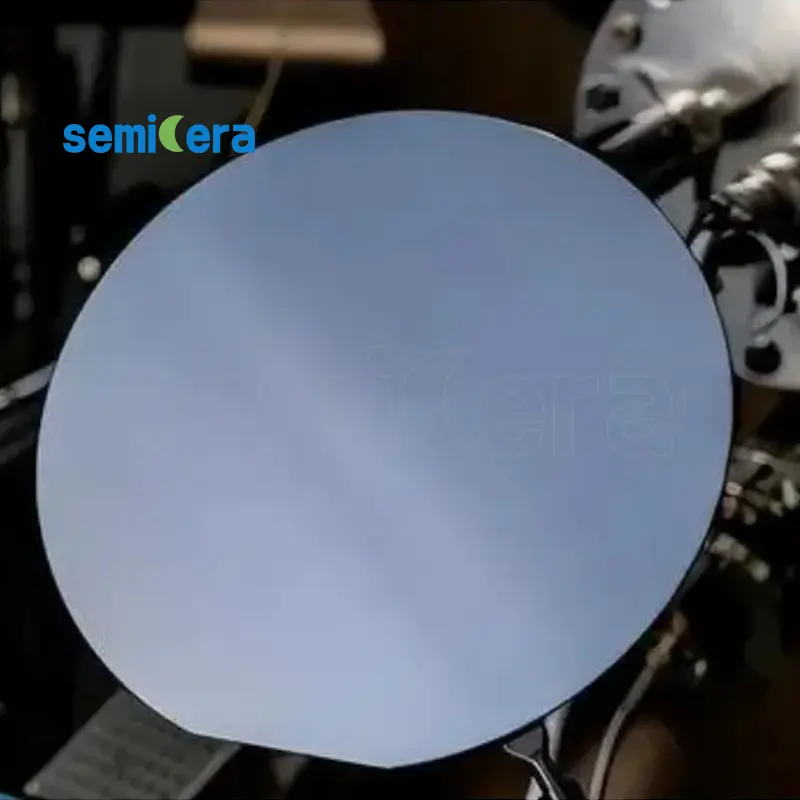
Półcesta proudly offers Ga2O3 Epitaxy, a state-of-the-art solution designed to push the boundaries of power electronics and optoelectronics. This advanced epitaxial technology leverages the unique properties of Gallium Oxide (Ga2O3) to deliver superior performance in demanding applications.
Key Features:
• Exceptional Wide Bandgap: Ga2O3 Epitaxy features an ultra-wide bandgap, allowing for higher breakdown voltages and efficient operation in high-power environments.
• High Thermal Conductivity: The epitaxial layer provides excellent thermal conductivity, ensuring stable operation even under high-temperature conditions, making it ideal for high-frequency devices.
• Superior Material Quality: Achieve high crystal quality with minimal defects, ensuring optimal device performance and longevity, especially in critical applications such as power transistors and UV detectors.
• Versatility in Applications: Perfectly suited for power electronics, RF applications, and optoelectronics, providing a reliable foundation for next-generation semiconductor devices.
Discover the potential of Ga2O3 Epitaxy with Semicera’s innovative solutions. Our epitaxial products are designed to meet the highest standards of quality and performance, enabling your devices to operate with maximum efficiency and reliability. Choose Semicera for cutting-edge semiconductor technology.
|
Rzeczy |
Produkcja |
Badania |
Atrapa |
|
Parametry kryształów |
|||
|
Polityp |
4H |
||
|
Błąd orientacji powierzchni |
4±0.15° |
||
|
Parametry elektryczne |
|||
|
Dopant |
azot typu N. |
||
|
Oporność |
0,015-0,025OHM · cm |
||
|
Parametry mechaniczne |
|||
|
Średnica |
150,0 ± 0,2 mm |
||
|
Grubość |
350 ± 25 µm |
||
|
Pierwotna płaska orientacja |
[1-100]±5° |
||
|
Pierwotna płaska długość |
47,5 ± 1,5 mm |
||
|
Wtórne mieszkanie |
Nic |
||
|
TTV |
≤5 µm |
≤10 µm |
≤15 µm |
|
LTV |
≤3 μm (5 mm*5 mm) |
≤5 μm (5 mm*5 mm) |
≤10 μm (5 mm*5 mm) |
|
Ukłon |
-15 μm ~ 15 μm |
-35 μm ~ 35 μm |
-45 μm ~ 45 μm |
|
Osnowa |
≤35 µm |
≤45 µm |
≤55 µm |
|
Chropowatość z przodu (SI-FACE) (AFM) |
RA ≤ 0,2 nm (5 μm*5 μm) |
||
|
Struktura |
|||
|
Gęstość mikropipe |
<1 ea/cm2 |
<10 ea/cm2 |
<15 ea/cm2 |
|
Zanieczyszczenia metalowe |
≤5E10atoms/cm2 |
Na |
|
|
BPD |
≤1500 EA/CM2 |
≤3000 EA/CM2 |
Na |
|
TSD |
≤500 EA/CM2 |
≤1000 EA/CM2 |
Na |
|
Jakość z przodu |
|||
|
Przód |
Si |
||
|
Wykończenie powierzchni |
SI-FACE CMP |
||
|
Cząsteczki |
≤60ea/wafel (rozmiar ≥0,3 μm) |
Na |
|
|
Zadrapania |
≤5EA/mm. Kumulatywna długość ≤ -diameter |
Skumulowana długość ≤2*średnica |
Na |
|
Skórka pomarańczowa/doły/plamy/prążki/pęknięcia/zanieczyszczenie |
Nic |
Na |
|
|
Płyty krawędziowe/wkładki/złamanie/sześciokątne płyty |
Nic |
||
|
Obszary politypowe |
Nic |
Obszar skumulowany ≤20% |
Obszar skumulowany ≤30% |
|
Przednie oznaczenie lasera |
Nic |
||
|
Jakość wstecz |
|||
|
Wstecz |
CMP-FACE CMP |
||
|
Zadrapania |
≤5EA/mm, kumulatywna długość ≤2*średnica |
Na |
|
|
Wady tylne (chipsy krawędziowe/wentylatory) |
Nic |
||
|
Chropowatość pleców |
RA ≤ 0,2 nm (5 μm*5 μm) |
||
|
Oznaczenie lasera z tyłu |
1 mm (od górnej krawędzi) |
||
|
Krawędź |
|||
|
Krawędź |
Ścięcie |
||
|
Opakowanie |
|||
|
Opakowanie |
Epi-gotowe z opakowaniem próżniowym Opakowanie kaseta z wieloma falami |
||
|
*Uwagi : „Na” oznacza, że brak wymienionych elementów, które nie wspomniane elementy mogą zapoznać się z pół-STD. |
|||


