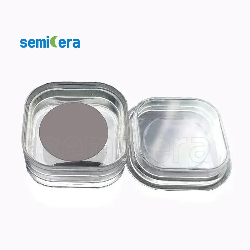
Półcesta is proud to present the Podłoże waflowe azotku aluminiowego 30 mm, a top-tier material engineered to meet the stringent demands of modern electronic and optoelectronic applications. Aluminum Nitride (AlN) substrates are renowned for their outstanding thermal conductivity and electrical insulation properties, making them an ideal choice for high-performance devices.
Key Features:
• Exceptional Thermal Conductivity: The Podłoże waflowe azotku aluminiowego 30 mm boasts a thermal conductivity of up to 170 W/mK, significantly higher than other substrate materials, ensuring efficient heat dissipation in high-power applications.
• High Electrical Insulation: With excellent electrical insulating properties, this substrate minimizes cross-talk and signal interference, making it ideal for RF and microwave applications.
• Mechanical Strength: The Podłoże waflowe azotku aluminiowego 30 mm offers superior mechanical strength and stability, ensuring durability and reliability even under rigorous operating conditions.
• Wszechstronne aplikacje: This substrate is perfect for use in high-power LEDs, laser diodes, and RF components, providing a robust and reliable foundation for your most demanding projects.
• Precision Fabrication: Semicera ensures that each wafer substrate is fabricated with the highest precision, offering uniform thickness and surface quality to meet the exacting standards of advanced electronic devices.
Maximize the efficiency and reliability of your devices with Semicera’s Podłoże waflowe azotku aluminiowego 30 mm. Our substrates are designed to deliver superior performance, ensuring that your electronic and optoelectronic systems operate at their best. Trust Semicera for cutting-edge materials that lead the industry in quality and innovation.
|
Rzeczy |
Produkcja |
Badania |
Atrapa |
|
Parametry kryształów |
|||
|
Polityp |
4H |
||
|
Błąd orientacji powierzchni |
4±0.15° |
||
|
Parametry elektryczne |
|||
|
Dopant |
azot typu N. |
||
|
Oporność |
0,015-0,025OHM · cm |
||
|
Parametry mechaniczne |
|||
|
Średnica |
150,0 ± 0,2 mm |
||
|
Grubość |
350 ± 25 µm |
||
|
Pierwotna płaska orientacja |
[1-100]±5° |
||
|
Pierwotna płaska długość |
47,5 ± 1,5 mm |
||
|
Wtórne mieszkanie |
Nic |
||
|
TTV |
≤5 µm |
≤10 µm |
≤15 µm |
|
LTV |
≤3 μm (5 mm*5 mm) |
≤5 μm (5 mm*5 mm) |
≤10 μm (5 mm*5 mm) |
|
Ukłon |
-15 μm ~ 15 μm |
-35 μm ~ 35 μm |
-45 μm ~ 45 μm |
|
Osnowa |
≤35 µm |
≤45 µm |
≤55 µm |
|
Chropowatość z przodu (SI-FACE) (AFM) |
RA ≤ 0,2 nm (5 μm*5 μm) |
||
|
Struktura |
|||
|
Gęstość mikropipe |
<1 ea/cm2 |
<10 ea/cm2 |
<15 ea/cm2 |
|
Zanieczyszczenia metalowe |
≤5E10atoms/cm2 |
Na |
|
|
BPD |
≤1500 EA/CM2 |
≤3000 EA/CM2 |
Na |
|
TSD |
≤500 EA/CM2 |
≤1000 EA/CM2 |
Na |
|
Jakość z przodu |
|||
|
Przód |
Si |
||
|
Wykończenie powierzchni |
SI-FACE CMP |
||
|
Cząsteczki |
≤60ea/wafel (rozmiar ≥0,3 μm) |
Na |
|
|
Zadrapania |
≤5EA/mm. Kumulatywna długość ≤ -diameter |
Skumulowana długość ≤2*średnica |
Na |
|
Skórka pomarańczowa/doły/plamy/prążki/pęknięcia/zanieczyszczenie |
Nic |
Na |
|
|
Płyty krawędziowe/wkładki/złamanie/sześciokątne płyty |
Nic |
||
|
Obszary politypowe |
Nic |
Obszar skumulowany ≤20% |
Obszar skumulowany ≤30% |
|
Przednie oznaczenie lasera |
Nic |
||
|
Jakość wstecz |
|||
|
Wstecz |
CMP-FACE CMP |
||
|
Zadrapania |
≤5EA/mm, kumulatywna długość ≤2*średnica |
Na |
|
|
Wady tylne (chipsy krawędziowe/wentylatory) |
Nic |
||
|
Chropowatość pleców |
RA ≤ 0,2 nm (5 μm*5 μm) |
||
|
Oznaczenie lasera z tyłu |
1 mm (od górnej krawędzi) |
||
|
Krawędź |
|||
|
Krawędź |
Ścięcie |
||
|
Opakowanie |
|||
|
Opakowanie |
Epi-gotowe z opakowaniem próżniowym Opakowanie kaseta z wieloma falami |
||
|
*Uwagi : „Na” oznacza, że brak wymienionych elementów, które nie wspomniane elementy mogą zapoznać się z pół-STD. |
|||


